A device and method for non-contact photoelectric detection of LED chips
An LED chip, non-contact technology, used in diode testing, single semiconductor device testing, etc., can solve the problems of inability to reflect individual differences, uneven current density, cumbersome testing process, etc., and achieve direct and accurate detection of photoelectric performance. Avoid glowing distracting effects
- Summary
- Abstract
- Description
- Claims
- Application Information
AI Technical Summary
Problems solved by technology
Method used
Image
Examples
Embodiment 1
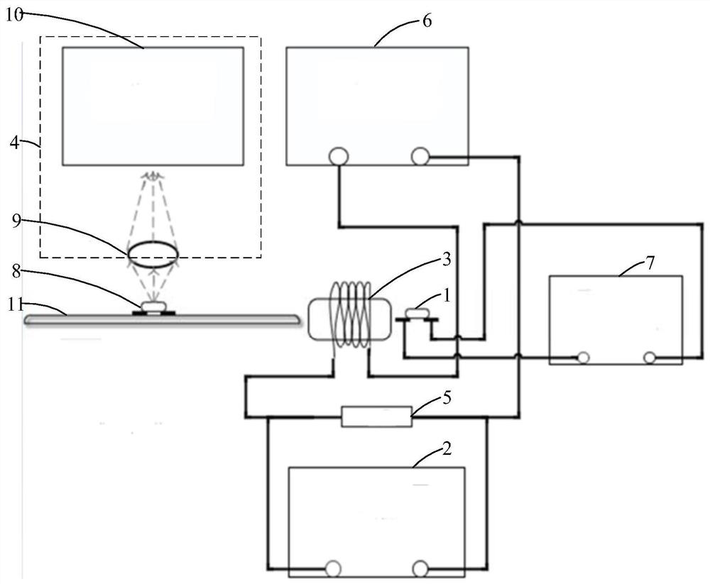
[0070] Please refer to figure 1 , Embodiment 1 of the present invention is:
[0071] A device for non-contact photoelectric detection of LED chips, such as figure 1 As shown, it includes a reference LED chip 1 , a shorting device, an oscilloscope 2 , an induction coil 3 , an optical measuring device 4 , a resistor 5 , a first current source 6 and a second current source 7 . Wherein, the oscilloscope 2 is connected in parallel at both ends of the resistor 5, the resistor 5, the first current source 6 and the induction coil 3 are connected in series to form a first closed loop, and the short circuit device is used to place the LED chip 8 to be tested and make the LED chip 8 to be tested The two electrodes are short-circuited to form a second closed loop. The reference LED chip 1 is connected in series with the second current source 7 to form a third closed loop. The second closed loop and the third closed loop are coaxial with the magnetic field direction of the induction coil ...
Embodiment 2
[0073] Please refer to figure 1 and figure 2 , the second embodiment of the present invention is:
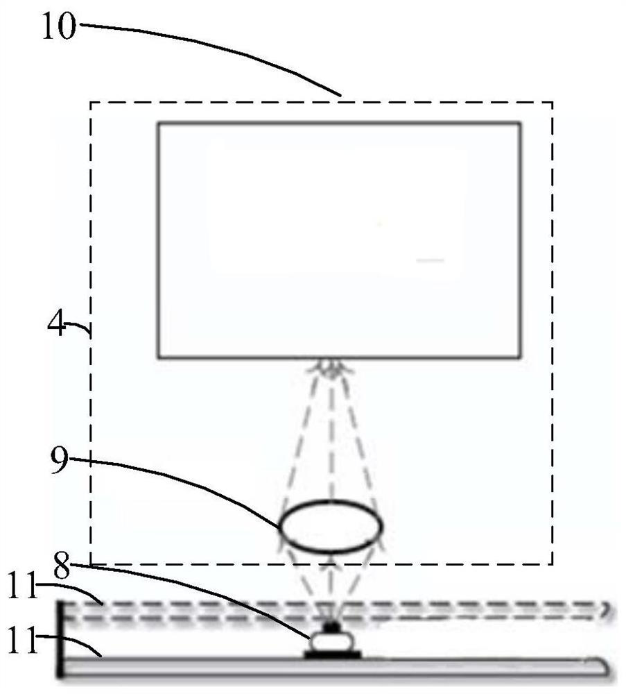
[0074] A device for non-contact photoelectric detection of LED chips, on the basis of the first embodiment above, such as figure 1 As shown, the shorting device includes a metal substrate 11, wherein the metal substrate 11 is used to simultaneously contact with the two electrodes of the LED chip 8 to be tested so that the two electrodes of the LED chip 8 to be tested are shorted to form a second closed loop.
[0075] In this example, if figure 2 As shown, the shorting device includes metal substrates 11 located on different sides and electrically connected to each other. Specifically, the metal substrates 11 on different sides are respectively used to contact corresponding electrodes on different sides of the LED chip 8 to be tested so that the two electrodes of the LED chip 8 to be tested are short-circuited to form a second closed loop. figure 2 The structural design sh...
Embodiment 3
[0076] Please refer to image 3 , the third embodiment of the present invention is:
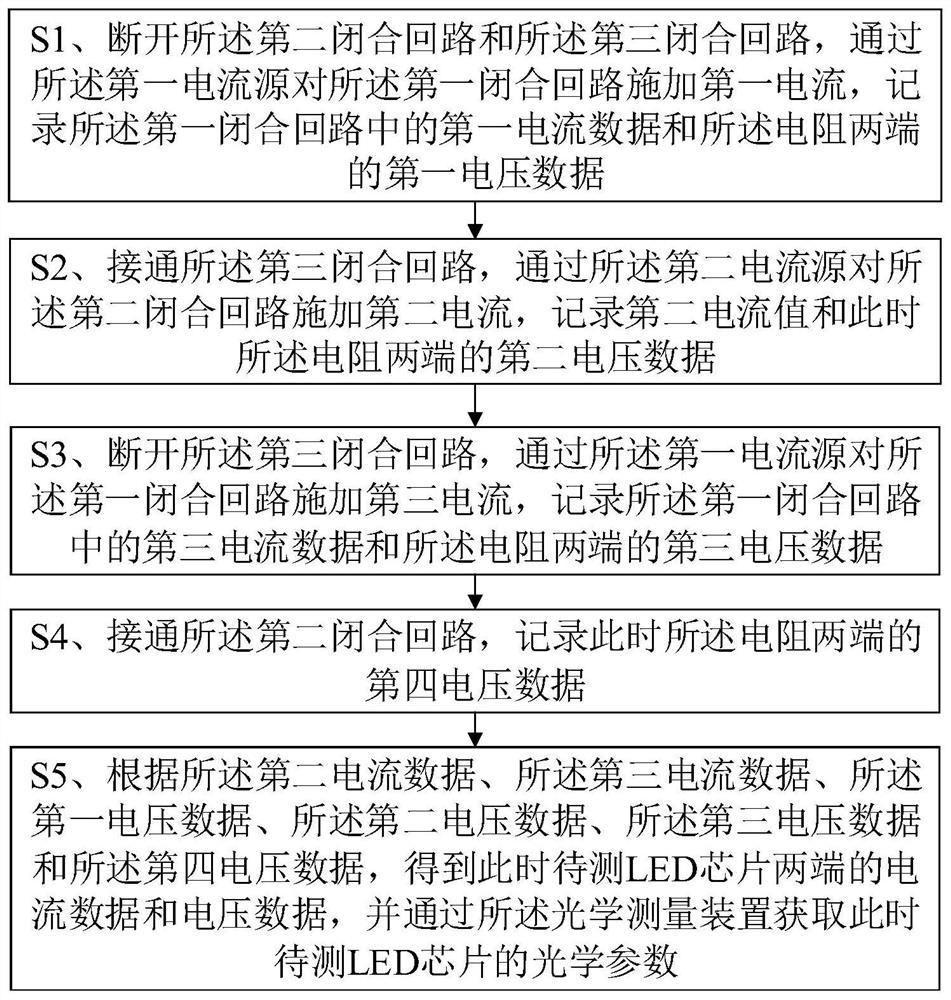
[0077] A method for non-contact photoelectric detection of LED chips, applied to a device for non-contact photoelectric detection of LED chips in Embodiment 1 or Embodiment 2, comprising steps:
[0078] S1, disconnect the second closed loop and the third closed loop, apply the first current to the first closed loop through the first current source 6, record the first current data in the first closed loop and the first voltage data at both ends of the resistor 5 ;
[0079] S2, connect the third closed loop, apply the second current to the second closed loop through the second current source 7, record the second current value and the second voltage data at the two ends of the resistor 5;
[0080] S3. Disconnect the third closed loop, apply a third current to the first closed loop through the first current source 6, and record the third current data in the first closed loop and the third volta...
PUM
 Abstract
Description
Claims
Application Information


