
Pixel driving circuit, OLED display panel and display device

A technology of pixel driving circuits and sub-pixels, which is applied in circuits, electrical components, electric solid-state devices, etc., can solve the problems of reduced brightness, difficulty in achieving ultra-high PPI, etc., and achieve the effect of improving pixel density.

Pending Publication Date: 2021-05-28
BOE TECH GRP CO LTD
View PDF5 Cites 1 Cited by
  • Summary
  • Abstract
  • Description
  • Claims
  • Application Information

AI Technical Summary

Problems solved by technology

At present, the traditional silicon-based OLED device adopts the structure of white light OLED and color film, but because the efficiency of white light OLED device is not as high as that of RGB OLED device, and the introduction of color film structure will lead to the decrease of brightness, so the structure of side-by-side RGB OLED sub-pixels can be used Significantly increased brightness
However, the structure of RGB OLED has three sub-pixels arranged side by side, making it difficult to achieve ultra-high PPI

Method used


Image

  • Pixel driving circuit, OLED display panel and display device
  • Pixel driving circuit, OLED display panel and display device
  • Pixel driving circuit, OLED display panel and display device

Examples


Embodiment Construction

[0022] The present application will be further described in detail below with reference to the accompanying drawings and embodiments. It should be understood that the specific embodiments described herein are only used to explain the related invention, but not to limit the invention. In addition, it should be noted that, for the convenience of description, only the parts related to the invention are shown in the drawings.

[0023] It should be noted that the embodiments in the present application and the features of the embodiments may be combined with each other in the case of no conflict. The present application will be described in detail below with reference to the accompanying drawings and in conjunction with the embodiments.

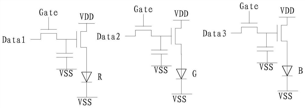
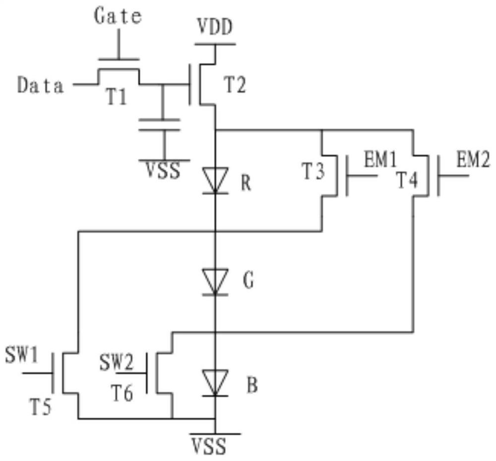
[0024] This embodiment provides a pixel driving circuit, including a data writing module, a driving module, a light-emitting device group, and an anode potential control module,

[0025] The data writing module is used for providing the data volt...


PUM


Abstract

The invention discloses a pixel driving circuit, an OLED display panel and a display device. The pixel driving circuit comprises a data write-in module, a driving module, a light-emitting device and an anode potential control module, and the data write-in module is used for providing data voltage to the driving module under the control of a gate driving signal; the driving module is used for driving a first light-emitting device or a second light-emitting device or a third light-emitting device in the light-emitting devices to emit light; and the anode potential control module is used for writing voltage into anodes of the light-emitting devices. According to the technical scheme provided by the embodiment of the invention, the pixel driving circuit is provided, and fewer transistors and capacitors are adopted on the provided pixel driving circuit, so that the pixel density of the display panel is improved.

Description

technical field [0001] The present invention generally relates to the field of display technology, and in particular, to a pixel driving circuit, an OLED display panel, and a display device. Background technique [0002] In recent years, silicon-based micro-displays have been developing in the direction of high PPI (Pixels Per Inch, pixel density). At present, the traditional silicon-based OLED device adopts the structure of white light OLED plus color film, but because the efficiency of white light OLED device is not as high as that of RGBOLED device, and the introduction of color film structure will reduce the brightness, so the structure of each sub-pixel side by side of RGB OLED can be used. Significantly improves brightness. However, the structure of RGB OLED has three sub-pixels arranged side by side, which makes it difficult to achieve ultra-high PPI. [0003] like figure 1 Shown is a drive circuit diagram of a sub-pixel structure arranged side by side in the prior...

Claims


Application Information

Patent Timeline
IPC IPC(8): G09G3/3225G09G3/3258H01L27/32
CPCG09G3/3225G09G3/3258H10K59/32
Inventor 袁丽君张粲丛宁王灿牛晋飞李伟张晶晶玄明花
Owner BOE TECH GRP CO LTD
Learn More