Semiconductor structure and forming method thereof

A technology of semiconductor and gate structure, applied in the field of semiconductor structure and its formation, can solve the problems of poor performance of semiconductor structure, achieve the effect of improving performance and heat dissipation

Pending Publication Date: 2021-05-28
SEMICON MFG INT (SHANGHAI) CORP +1
View PDF17 Cites 0 Cited by
  • Summary
  • Abstract
  • Description
  • Claims
  • Application Information

AI Technical Summary

Problems solved by technology

[0006] However, semiconductor structures formed by existing methods have poor performance

Method used


Image

  • Semiconductor structure and forming method thereof
  • Semiconductor structure and forming method thereof
  • Semiconductor structure and forming method thereof

Examples


Embodiment Construction

[0034] As mentioned in the background, the performance of semiconductor structures formed by existing methods is poor. The following will describe in detail in conjunction with the accompanying drawings.

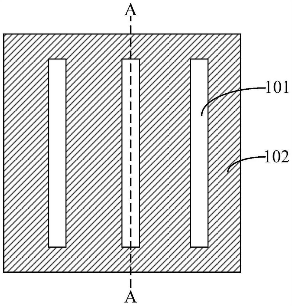
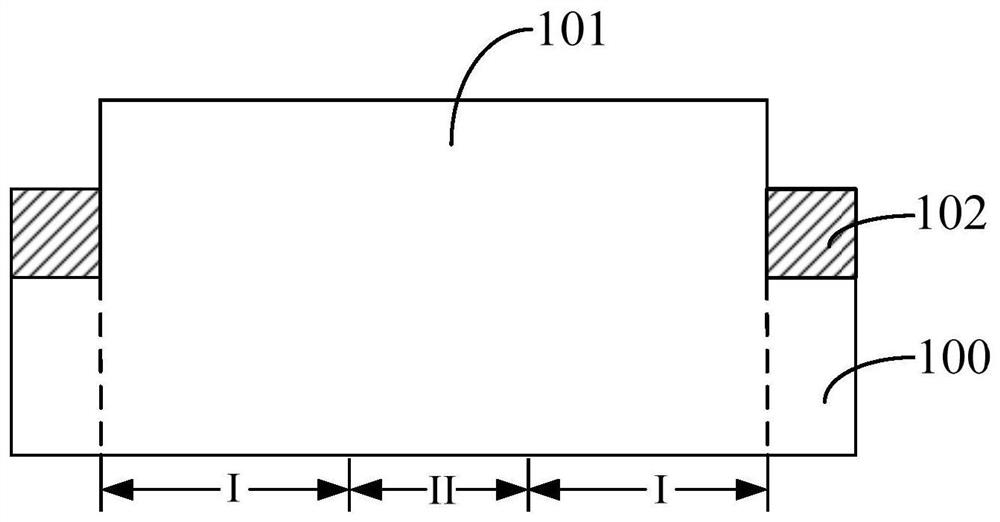
[0035] Please refer to figure 1 and figure 2 , figure 2 Yes figure 1 A schematic cross-sectional view along the A-A direction, a substrate 100 is provided, and the substrate 100 has fins 101 extending along a first direction, and the fins 101 include a plurality of first regions I and at least one The second zone II, the second zone II is located between two adjacent first zones I, the first zone I and the second zone II are arranged along the first direction; in the A first isolation layer 102 is formed on the substrate 100 , the first isolation layer 102 covers part of the sidewall of the fin 101 , and the surface of the first isolation layer 102 is lower than the top surface of the fin 101 .

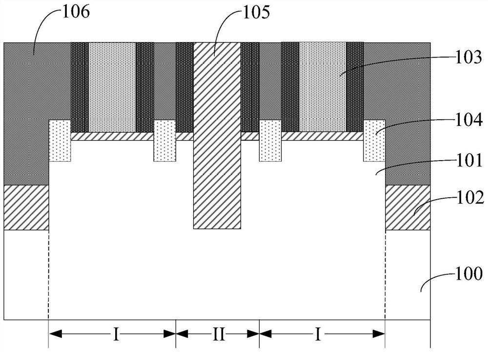
[0036] Please refer to image 3 ,It should be noted, image 3 and ...


PUM


Abstract

The invention discloses a semiconductor structure and a forming method thereof, and the method comprises the steps: providing a substrate which is provided with fin parts, wherein the fin parts extend in a first direction, the fin parts comprise a plurality of first regions and at least one second region, and the second region is located between two adjacent first regions; forming a first isolation layer on the substrate, wherein the first isolation layer covers part of the side walls of the fin parts, and the surface of the first isolation layer is lower than the top surfaces of the fin parts; forming first grid structures crossing the fin parts and source-drain doped regions located in the fin parts on the two sides of the first grid structures on the first regions respectively, wherein the first grid structures cover part of the side walls and the top surfaces of the fin parts; forming a second isolation layer in the second region, wherein the second isolation layer penetrates through the fin parts along a second direction; and forming a second grid structure on the second isolation layer. The second grid structure is formed on the second isolation layer, and a metal material in the second grid structure has good heat conduction performance, so that heat energy generated by the semiconductor structure can be timely and effectively led out, and the performance of the semiconductor structure is effectively improved.

Description

technical field [0001] The invention relates to the technical field of semiconductor manufacturing, in particular to a semiconductor structure and a forming method thereof. Background technique [0002] As the integration level of semiconductor devices increases, the critical dimensions of transistors continue to shrink. However, as the size of the transistor decreases sharply, the thickness of the gate dielectric layer and the operating voltage cannot be changed accordingly, which makes it more difficult to suppress the short channel effect and increases the channel leakage current of the transistor. [0003] The gate of the Fin Field-Effect Transistor (FinFET) has a forked 3D structure similar to a fish fin. The channel of the FinFET protrudes from the surface of the substrate to form a fin, and the gate covers the top surface and side walls of the fin, so that the inversion layer is formed on each side of the channel, and the connection of the circuit can be controlled o...

Claims


Application Information

Patent Timeline
Patent Type & Authority Applications(China)
IPC IPC(8): H01L21/336H01L29/78
CPCH01L29/66803H01L29/785
Inventor 周飞
Owner SEMICON MFG INT (SHANGHAI) CORP
Why Eureka
Try Eureka