
Preparation method of bulk acoustic wave resonator and bulk acoustic wave resonator

A technology of bulk acoustic wave resonators and sacrificial layers, applied in electrical components, impedance networks, etc., can solve the problems of cumbersome process steps of bulk acoustic wave resonators and low yield of bulk acoustic wave resonators, and reduce the number of etching times and simplify the process The effect of steps

Pending Publication Date: 2021-06-11
SUZHOU HUNTERSUN ELECTRONICS CO LTD
View PDF3 Cites 2 Cited by
  • Summary
  • Abstract
  • Description
  • Claims
  • Application Information

AI Technical Summary

Problems solved by technology

[0003] In the process of forming a bulk acoustic wave resonator in the prior art, in order to reduce the energy loss of the bulk acoustic wave, a structure is provided inside the bulk acoustic wave resonator to avoid the energy loss of the acoustic wave. In the prior art, in the process of preparing the bulk acoustic wave resonator, it is necessary to On the first surface side of the piezoelectric layer and on the second surface of the piezoelectric layer opposite to the first surface, an etching process is used to form a structure to avoid the loss of acoustic wave energy. The above-mentioned preparation method uses a mask plate and an etching process. Too many times lead to cumbersome process steps for preparing bulk acoustic wave resonators, and the yield rate of bulk acoustic wave resonators is not high

Method used


Image

  • Preparation method of bulk acoustic wave resonator and bulk acoustic wave resonator
  • Preparation method of bulk acoustic wave resonator and bulk acoustic wave resonator
  • Preparation method of bulk acoustic wave resonator and bulk acoustic wave resonator

Examples


Embodiment Construction

[0058] The present invention will be further described in detail below in conjunction with the accompanying drawings and embodiments. It should be understood that the specific embodiments described here are only used to explain the present invention, but not to limit the present invention. In addition, it should be noted that, for the convenience of description, only some structures related to the present invention are shown in the drawings but not all structures.

[0059] As mentioned in the background art above, in the prior art, too many times of etching are used in the process of manufacturing the bulk acoustic wave resonator, resulting in complicated process steps for manufacturing the bulk acoustic wave resonator. The reason is that in the prior art, in the process of preparing a bulk acoustic wave resonator, it is necessary to use the geometric pattern on the mask plate to transfer the pattern to the substrate covering the first surface side of the piezoelectric layer t...


PUM

PropertyMeasurementUnit
widthaaaaaaaaaa
thicknessaaaaaaaaaa
thicknessaaaaaaaaaa

Abstract

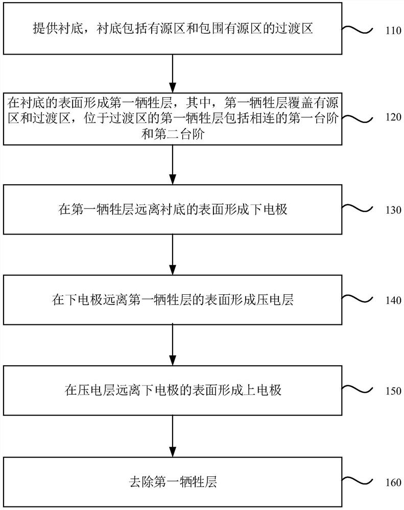
The invention discloses a preparation method of a bulk acoustic wave resonator and the bulk acoustic wave resonator. The preparation method of the bulk acoustic wave resonator comprises the following steps: providing a substrate, wherein the substrate comprises an active region and a transition region surrounding the active region; forming a first sacrificial layer on the surface of the substrate, wherein the first sacrificial layer covers the active region and the transition region; the first sacrificial layer in the transition region comprises a first step and a second step which are connected; the height of the first step is larger than that of the first sacrificial layer in the active region; and the height of the second step is smaller than that of the first sacrificial layer in the transition region; and the height of the second step is smaller than that of the first sacrificial layer in the active region; forming a lower electrode on the surface, away from the substrate, of the first sacrificial layer; forming a piezoelectric layer on the surface, away from the first sacrificial layer, of the lower electrode; forming an upper electrode on the surface, away from the lower electrode, of the piezoelectric layer; and removing the first sacrificial layer. According to the technical scheme provided by the embodiment of the invention, the process steps for preparing the bulk acoustic wave resonator are simplified, and the yield of the bulk acoustic wave resonator is improved.

Description

technical field [0001] Embodiments of the present invention relate to the technical field of semiconductors, and in particular to a method for preparing a bulk acoustic wave resonator and the bulk acoustic wave resonator. Background technique [0002] Bulk Acoustic Wave (BAW) resonators have excellent characteristics such as small size, high resonance frequency, high quality factor, and large power capacity, and play an important role in the field of communication. [0003] In the process of forming a bulk acoustic wave resonator in the prior art, in order to reduce the energy loss of the bulk acoustic wave, a structure is provided inside the bulk acoustic wave resonator to avoid the energy loss of the acoustic wave. In the prior art, in the process of preparing the bulk acoustic wave resonator, it is necessary to On the first surface side of the piezoelectric layer and on the second surface of the piezoelectric layer opposite to the first surface, an etching process is used...

Claims


Application Information

Patent Timeline
Patent Type & Authority Applications(China)
IPC IPC(8): H03H9/17H03H3/02H03H9/02H03H9/05H03H9/09
CPCH03H9/17H03H9/02H03H3/02H03H9/09H03H9/05
Inventor 唐滨唐兆云王家友赖志国杨清华
Owner SUZHOU HUNTERSUN ELECTRONICS CO LTD
Learn More