Array substrate, manufacturing method thereof and display panel
A technology for array substrates and substrate substrates, which is applied in the manufacture of semiconductor/solid-state devices, instruments, semiconductor devices, etc., can solve the problems such as the decrease of the aperture ratio of the display panel, and achieve the effects of reducing light leakage, uniform electric field, and increasing the aperture ratio
- Summary
- Abstract
- Description
- Claims
- Application Information
AI Technical Summary
Problems solved by technology
Method used
Image


Examples
Embodiment 1
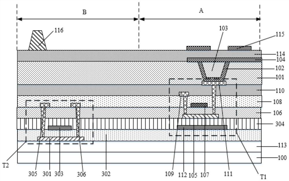
[0053] Refer figure 1 The cross-sectional view of the first array substrate of the embodiment of the present invention is shown; figure 2 A cross-sectional view of the second array substrate of the embodiment of the present invention is shown; image 3 A cross-sectional view of a third array substrate according to an embodiment of the present invention is shown; Figure 4A cross-sectional view of a fourth array substrate according to an embodiment of the present invention is shown;
[0054] In the embodiment of the present invention, an array substrate includes: a substrate substrate 100; a first transistor T1 provided on the side of the substrate board 100, the first transistor T1 is located within the display area A of the array substrate; covering the first transistor The flat layer 101 of T1, the flat layer 101 has a first through hole of T1; a first electrode layer 102 disposed within the first through hole, the first electrode layer 102 and the drain connection in the first tr...
Embodiment 2
[0110] Embodiments of the present invention also provide a display panel, including an array substrate in the above-described embodiment.
[0111] The display panel can be displayed on the LCD (Liquid Crystal Display, the LCD) display panel, or when the display panel is the LCD display panel, the display panel also includes an array The substrate is relatively disposed, the liquid crystal layer between the array substrate and the color film substrate is located on the side of the color film substrate from the array substrate, and the second polarizing sheet located on the array substrate from the color film substrate. Wait.
[0112] In practical applications, the display panel can be applied to: mobile phones, tablets, TVs, displays, laptops, navigators, etc. have any product or components with display functions.
[0113] In the embodiment of the present invention, by providing a filling layer in the first recess of the first electrode layer to fill the first groove, the second el...
Embodiment 3
[0115] Figure 5 A flow diagram of a method of fabricating an array substrate according to an embodiment of the present invention may comprise the next step:
[0116] Step 501, a first transistor is formed on one side of the substrate substrate, the first transistor located within the display area of the array substrate.
[0117] In the embodiment of the present invention, the array substrate includes a display area A and a GOA region B, providing a substrate 100, forming a first transistor T1 on one side of the substrate substrate 100 of the display area A, and the first transistor T1 can be The top gate type transistor may also be a bottom gate transistor.
[0118] When the first transistor T1 is a top gate transistor, figure 1 As shown, the formation process of the first transistor T1 is: forming a first active layer 105 on one side of the substrate substrate 100; forming a first gate insulating layer 106 covering the first active layer 105; in the first gate The insulating l...
PUM
| Property | Measurement | Unit |
|---|---|---|
| Thickness | aaaaa | aaaaa |
| Thickness | aaaaa | aaaaa |
| Thickness | aaaaa | aaaaa |
Abstract
Description
Claims
Application Information