A peel-off method for pi flexible substrates based on a silk-mesh-like substrate layer, flexible substrates and OLEDs

A flexible substrate and substrate layer technology, applied in the direction of organic semiconductor devices, electric solid devices, semiconductor devices, etc., can solve problems such as complex operation process, inability to contact skin, damage to flexible OLED, etc., and achieve simple operation process without affecting integrity , The effect of reducing the bonding area

Active Publication Date: 2022-05-20
HUAZHONG UNIV OF SCI & TECH
View PDF9 Cites 0 Cited by
  • Summary
  • Abstract
  • Description
  • Claims
  • Application Information

AI Technical Summary

Problems solved by technology

This method is complicated to operate and the equipment is expensive. The high-temperature laser will cause certain damage to the flexible OLED. At the same time, the scanning size of the laser is also limited. At present, it is still impossible to prepare large-size flexible displays.
(2) Physical peeling generally uses mechanical equipment or manual mechanical peeling. The principle and operation of this method are simple, but if there is no special process, due to the strong adhesion between PI and glass, it is easy to tear directly by physical peeling. and damage flexible OLED optics
However, the above two chemical liquids that corrode glass or stainless steel are very dangerous and cannot be in contact with the skin or inhaled into the respiratory tract, and will also damage and affect flexible OLEDs.

Method used


Image

  • A peel-off method for pi flexible substrates based on a silk-mesh-like substrate layer, flexible substrates and OLEDs
  • A peel-off method for pi flexible substrates based on a silk-mesh-like substrate layer, flexible substrates and OLEDs
  • A peel-off method for pi flexible substrates based on a silk-mesh-like substrate layer, flexible substrates and OLEDs

Examples


preparation example Construction

[0076] The preparation method of the substrate film in the step (1) is sol-gel technology, dip coating method, CVD, PVD, liquid phase deposition method, electroevaporation, sputtering, silk screen printing and the like.

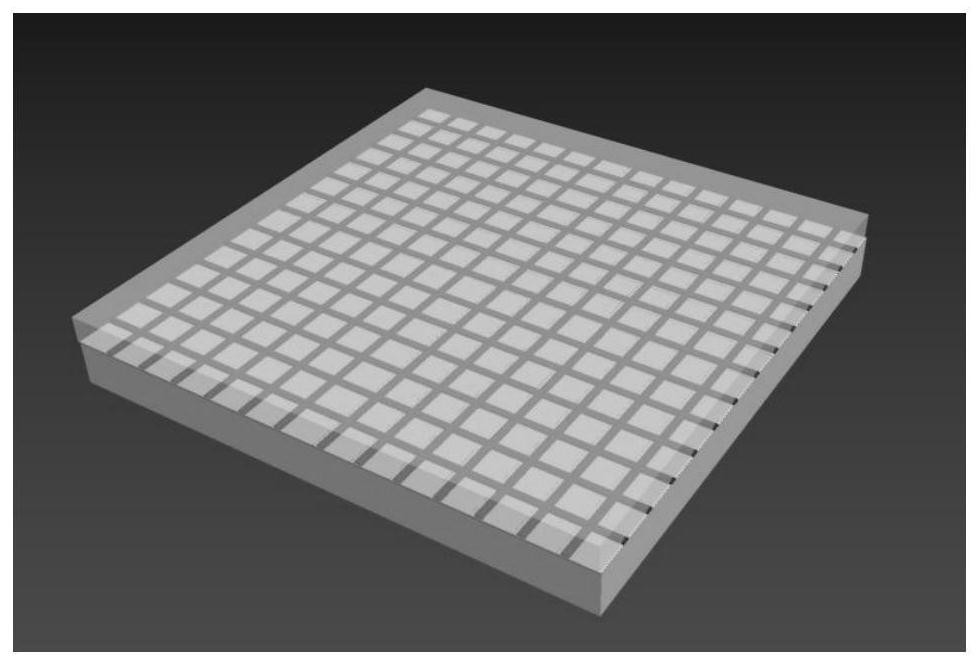
[0077] In the step (1), the screen pattern of the screen-like substrate layer is any pattern such as a square grid, a rhombus grid, a circle grid, a straight line grid, a curved grid, a circuit pattern, and a calligraphy and painting pattern.

[0078] In the step (1), the thickness of the wire mesh substrate layer is controlled within 10nm to 900um. The screen size is defined by line width and area ratio (screen area / substrate area), the line width is controlled from 1nm to 100um, and the area ratio is 0.01% to 99%.

[0079] In the step (2), a polyimide thin film PI flexible substrate is prepared on the screen-like substrate layer by means of spin coating, scraping coating and casting.

[0080] The step (3) prepares an organic optoelectronic device and packa...

Embodiment 1

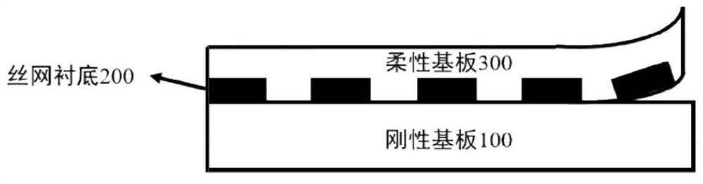
[0086] Embodiment 1: A PI (polyimide) flexible substrate peeling process based on silicon nitride mesh substrate layer technology.

[0087] Step (1): preparing a silicon nitride wire mesh substrate layer on the glass substrate;

[0088] The substrate material in step (1) is a glass substrate, which can also be replaced with one of ceramics and metal.

[0089] The material for depositing the screen-like substrate layer in step (1) is silicon nitride.

[0090]The thickness of the silicon nitride wire mesh substrate layer in step (1) is 230nm-290nm.

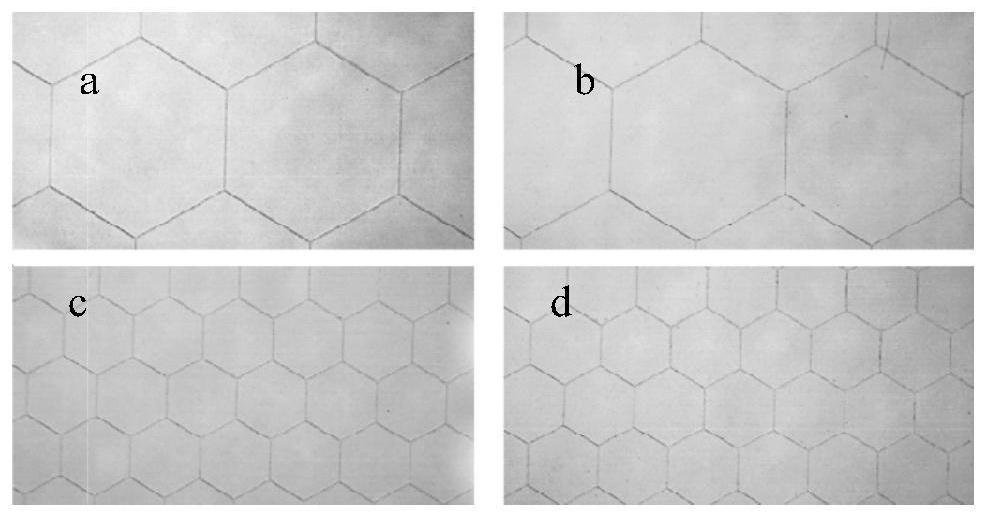
[0091] The pattern of the screen-like substrate layer in step (1) is selected as a hexagonal grid, and the line width of the screen is 200 μm-5 μm, 200 μm-10 μm, 500 μm-5 μm, and 500 μm-10 μm. . The area ratios were 0.494%, 0.975%, 0.0199%, and 0.0386%, respectively.

[0092] The screen-like substrate structure in step (1) is prepared by first photolithography and then deposition process:

[0093] Carry out pretreatment on the ...


PUM

PropertyMeasurementUnit
thicknessaaaaaaaaaa
thicknessaaaaaaaaaa
thicknessaaaaaaaaaa

Abstract

The invention discloses a PI flexible substrate stripping method based on a screen-like substrate layer, a flexible substrate and an OLED, and belongs to the field of flexible OLED preparation. The present invention adds a layer of screen-like substrate layer between the PI flexible substrate and the rigid substrate, and the difference in adhesion between the screen-shaped substrate layer and the PI flexible substrate to the rigid substrate changes the adhesion of the PI flexible substrate; in addition, the silk The concave-convex structure formed by the mesh substrate layer causes the flexible substrate attached to it to have a gap with the rigid substrate at the border of the screen. While changing the state of the bottom surface of the PI flexible substrate, it reduces the bonding area between the flexible substrate and the rigid substrate, and also The peeling force between the PI flexible substrate and the rigid substrate can be further adjusted to realize the simple and convenient peeling of the flexible substrate from the rigid substrate by means of physics, solution immersion or ultrasonic vibration. The peeling method is simple and the peeling effect is stable without affecting the PI flexible substrate. integrity.

Description

technical field [0001] The invention belongs to the field of flexible OLED preparation, and more specifically relates to a method for peeling off a PI flexible substrate based on a screen-like substrate layer, a flexible substrate and an OLED. Background technique [0002] Flexible OLED (Organic Electroluminesence Display, organic electroluminescence display) has outstanding performance due to its unique self-illumination, good viewing angle, fast response, heat and low temperature resistance, shock resistance without falling, thin and bendable, power saving and cost saving. Advantages and good user experience, the demand is showing explosive growth. The preparation of flexible OLEDs requires the preparation of PI (Polyimide, polyimide) flexible substrates on the surface of glass substrates. Films made of PI materials have high temperature resistance, good mechanical properties, good flexibility, dielectric constant, and transparency. properties, so it has become the most w...

Claims


Application Information

Patent Timeline
Patent Type & Authority Patents(China)
IPC IPC(8): H01L51/56H01L27/32
CPCH10K59/10H10K71/80H10K59/1201H10K71/851H10K71/00Y02E10/549
Inventor 屠国力吕晓煜刘相富
Owner HUAZHONG UNIV OF SCI & TECH
Why Eureka
Try Eureka