Connection probe, preparation method of connection probe and use of connection probe in microelectrode array connection

A technology for microelectrode arrays and connecting probes, applied to electrodes, internal electrodes, head electrodes, etc., can solve problems such as affecting the performance and life of microelectrode arrays, damaging the welding ends of microelectrode arrays, increasing manufacturing difficulty and cost, etc. , to achieve the effect of reversible connection, good universality and wide range

Active Publication Date: 2018-06-19
SHENZHEN INST OF ADVANCED TECH
View PDF13 Cites 7 Cited by
  • Summary
  • Abstract
  • Description
  • Claims
  • Application Information

AI Technical Summary

Problems solved by technology

However, this kind of probe card generally needs to be customized, and when it acts on a high-density microelectrode array, the size of the probe card will become very small, which greatly increases the difficulty and cost of production, and the price is very expensive. The probe of the probe card is generally made of hard material. When it is used to test the flexible high-density microelectrode array, it may damage the welding end of the microelectrode array and affect the performance and life of the microelectrode array.

Method used


Image

  • Connection probe, preparation method of connection probe and use of connection probe in microelectrode array connection

Examples


Embodiment 1

[0073] This embodiment provides a ligation probe and a preparation method thereof, the method comprising:

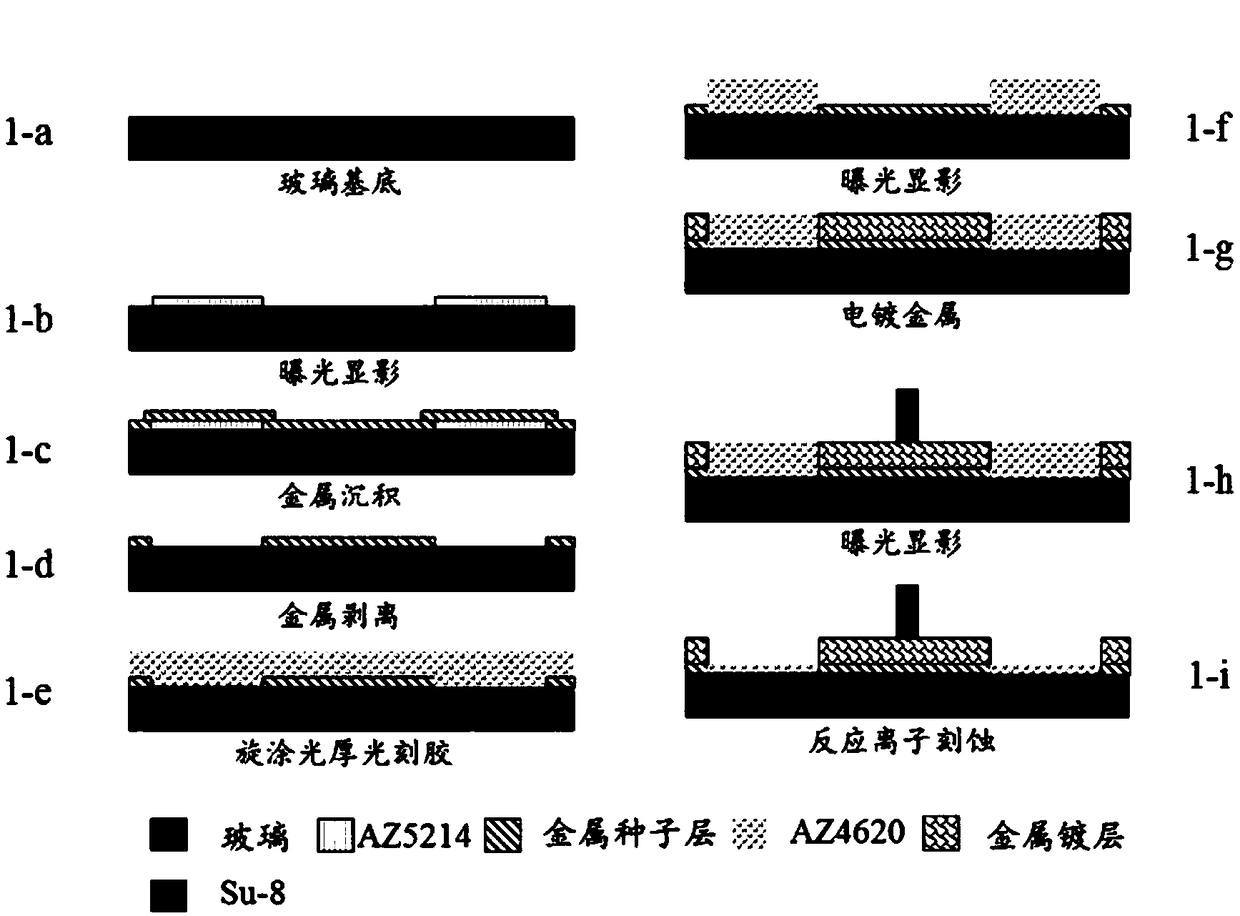
[0074] (1) Prepare the substrate: select a glass sheet with better dielectric properties as the substrate, and use it after cleaning (see figure 1 1-a) in.

[0075] (2) Exposure and development: Spin-coat a layer of photoresist AZ5214 on the substrate with a thickness of 3-5 microns. After heating and curing, use the first layer of mask as a mask for exposure and development (see figure 1 1-b) in.

[0076] (3) Metal deposition and metallic glass: the metal coating process is carried out on the sample after photolithography, and the Cr / Au metal layer of 20nm / 100nm is completed, and the target metal pattern is obtained by lift-off (see figure 1 1-c and 1-d in )

[0077] (4) Spin-coat light-thick photoresist, exposure and development, and electroplating metal: Next, spin-coat AZ4620 photoresist of 7-8 microns, expose and develop the metal of the probe part, and use the t...

Embodiment 2

[0082] Except not carrying out step (5) the step of spin-coating SU-8, other methods and conditions are identical with embodiment 1.

Embodiment 3

[0084] This embodiment provides a ligation probe and a preparation method thereof, the method comprising:

[0085] (1) Spin-coat AZ5214 photoresist with a thickness of 3 μm on the substrate, heat and cure it, then use a mask for exposure and development, and then deposit a 20nm Cr layer and a 100nm Au layer on the entire substrate area successively. This 120nm thick composite layer As a metal seed layer, the photoresist is stripped to form a metal seed layer arranged at intervals on the substrate;

[0086](2) Spin-coat AZ4620 photoresist on the entire substrate area, then expose the metal seed layer by exposure and development, use the photoresist as a mask, and electroplate on the metal seed layer to obtain a 7 μm thick metal coating, the metal seed layer and The metal plating layers jointly form array units arranged at intervals;

[0087] Wherein, the thickness of the AZ4620 photoresist is 7 μm to 8 μm, which is the same as the thickness of the array unit;

[0088] (2)'Spi...


PUM


Abstract

The present invention discloses a connection probe, a preparation method of the connection probe and the use of the connection probe in the microelectrode array connection, and belongs to the microelectrode array technology field. The connection probe of the present invention comprises a pedestal and the array units which are located on the pedestal and are arranged at intervals, and each array unit comprises the metal seed layers and a metal plating layer from bottom to top. According to the present invention, by utilizing a conventional micro-electro mechanical system (MEMS) technology to design innovatively, the problems that a high-density microelectrode array is difficult to carry out the electrical tests and the reliability tests, or the microelectrode array is damaged during the test process are solved, by utilizing the characteristics that an MEMS is high in processing and preparation precision, is miniature, etc., the probe used for a high-density flexible microelectrode testcan be prepared, and a lossless test effect can be realized. Moreover, the usage of the connection probe of the present invention is reversible, the probe can be taken off to be used repeatedly aftertests.

Description

technical field [0001] The invention belongs to the technical fields of microelectrode array technology, microelectromechanical system and implanted neural interface, and relates to a connection probe, its preparation method and its application in microelectrode array connection, especially to a connection probe, its preparation Method and use in connection of implantable flexible neurostimulation electrodes. Background technique [0002] Generally, the flexible microelectrode array is composed of stimulation points, wires, and pads. The finished flexible microelectrode array needs to be electroplated or electrically tested, so that the flexible microelectrode array must be connected to external electrical equipment, such as electroplating. ChemStation, electrical testing requires connection to test circuit. [0003] In order to establish a connection between the flexible microelectrode array and external electrical equipment, the general method is to solder the electrode t...

Claims


Application Information

Patent Timeline
Patent Type & Authority Applications(China)
IPC IPC(8): A61N1/36A61N1/05
CPCA61N1/0543A61N1/36046A61N1/36125
Inventor 孙滨吴天准夏凯付博文
Owner SHENZHEN INST OF ADVANCED TECH
Why Eureka
Try Eureka