Power amplification module

A power amplifier module and power stage technology, applied in power amplifiers, amplifiers, radio frequency amplifiers, etc., can solve problems such as larger deviation of impedance conversion circuits, longer signal paths, and increased parasitic resistances.

Active Publication Date: 2021-06-22
MURATA MFG CO LTD
View PDF7 Cites 0 Cited by
  • Summary
  • Abstract
  • Description
  • Claims
  • Application Information

AI Technical Summary

Problems solved by technology

As a result, depending on the transistor, the signal path from the signal output port to the impedance conversion circuit becomes longer and the parasitic resistance increases
In addition, the variation in the length from the signal output port of the transistor to the impedance conversion circuit becomes large

Method used


Image

  • Power amplification module
  • Power amplification module
  • Power amplification module

Examples


no. 1 example

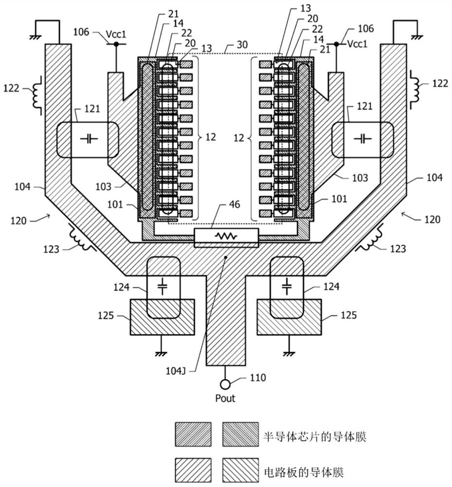
[0069] refer to Figure 1 to Figure 5 The accompanying drawings illustrate the power amplifying module of the first embodiment.

[0070] figure 1 It is a diagram showing the positional relationship in plan view of a plurality of constituent elements of the power stage amplifying circuit and the output impedance converting circuit of the power amplifying module of the first embodiment. The power amplifying module of the first embodiment has a semiconductor chip and a circuit board. exist figure 1 In this method, relatively thick shading is given to the conductor film formed on the semiconductor chip, and relatively light shading is given to the conductor film formed on the circuit board.

[0071] First, the structure of a semiconductor chip will be described. The semiconductor chip includes a substrate made of a semiconductor, and two transistor columns 12 arranged on the substrate. Each of the two transistor columns 12 includes a plurality (for example, 12) of power stage ...

no. 2 example

[0123] Next, refer to Figure 10 as well as Figure 11 , to describe the power amplifying module of the second embodiment. Hereinafter, for the power amplifying module ( Figure 1 to Figure 5 Accompanying drawing) common structure, omit description.

[0124] Figure 10 It is a diagram showing the positional relationship in plan view of a plurality of constituent elements of the power stage amplifying circuit and the output impedance converting circuit of the power amplifying module of the second embodiment. exist Figure 10 in, also with figure 1 Similarly, relatively thick shadows are added to the conductor film provided on the semiconductor chip 10, and relatively thick shadows are applied to the conductor film provided on the circuit board 100 ( figure 2 ) is shaded relatively lightly.

[0125] In the first embodiment, the first bump 21 and the collector wiring 14 ( figure 1 ) are connected in a direct current manner. In contrast, in the second embodiment, the fir...

no. 3 example

[0135] Next, refer to Figure 12 , to describe the power amplifying module of the third embodiment. Below, for Figure 1 to Figure 5 The common structure of the power amplifying module of the first embodiment shown in the accompanying drawings is omitted.

[0136] Figure 12 It is a diagram showing the positional relationship in plan view of a plurality of constituent elements of the power stage amplifying circuit and the output impedance converting circuit of the power amplifying module of the third embodiment. In the first embodiment, the two transistor columns 12 are arranged along two opposing sides of the rectangular convex polygon 30 . In contrast, in the third embodiment, two transistor columns 12 are arranged along two sides of a square convex polygon 30 adjacent to each other.

[0137] The respective collector mesas 20 of the power stage transistors 13 have a long shape in a direction forming 45° with respect to the sides of the convex polygon 30 in plan view. Th...


PUM


Abstract

Provided is a power amplification module capable of suppressing an increase in the length of a region occupied by a transistor row, and suppressing an increase in parasitic resistance from a transistor to an impedance conversion circuit and an increase in variation in parasitic inductance. A semiconductor chip includes a plurality of transistor rows. Corresponding to the plurality of transistor rows, a first bump connected to a collector of the transistor is arranged, and a second bump connected to an emitter is arranged. The transistor rows are arranged along sides of a convex polygon. A first land and a second land provided in a circuit board are connected to the first bump and the second bump, respectively. A first impedance conversion circuit connects the first land and the signal output terminal. A plurality of transistors in the transistor row are grouped into a plurality of groups, and the first impedance conversion circuit includes a reactance element arranged for each of the groups.

Description

technical field [0001] The invention relates to a power amplification module. Background technique [0002] A plurality of transistors connected in parallel to each other are used in the final stage (power stage) of the high-frequency power amplifying circuit of the multistage structure. An impedance conversion circuit for impedance matching is inserted between the amplifying circuit of the power stage and the load. In general, an impedance conversion circuit that converts the output impedance of the power stage amplifier circuit to high impedance is used. [0003] In order to increase the output of the power amplifier circuit, it is necessary to flow a large current through the signal path from the collector as the signal output port of the transistor group to the input port of the impedance conversion circuit. Losses in the signal path are proportional to the product of the square of the current and the parasitic resistance. Therefore, as the flowing current increases, ...

Claims


Application Information

Patent Timeline
Patent Type & Authority Applications(China)
IPC IPC(8): H03F3/20
CPCH03F3/20H03F1/565H03F3/195H03F3/602H03F2200/451H05K1/181H05K2201/10166H01L23/5227H01L2223/6655H01L23/66H01L23/5223H01L2224/17H01L2224/16225H03F3/213H01L2924/30111H03F2200/222H01L2224/16227H01L2924/1421H01L24/16
Inventor 近藤将夫竹中干一郎田中聪筒井孝幸
Owner MURATA MFG CO LTD
Why Eureka
Try Eureka