Wafer back alignment method, wafer back alignment equipment and photoetching machine
A technology of alignment equipment and backside alignment, which is applied in the field of wafer backside alignment, wafer backside alignment equipment and lithography machines, which can solve the problems of alignment efficiency, low alignment accuracy, and computational accuracy. It can improve the alignment efficiency and alignment accuracy, improve the calculation accuracy, and reduce the operation steps.
- Summary
- Abstract
- Description
- Claims
- Application Information
AI Technical Summary
Problems solved by technology
Method used
Image

Examples
Embodiment 1
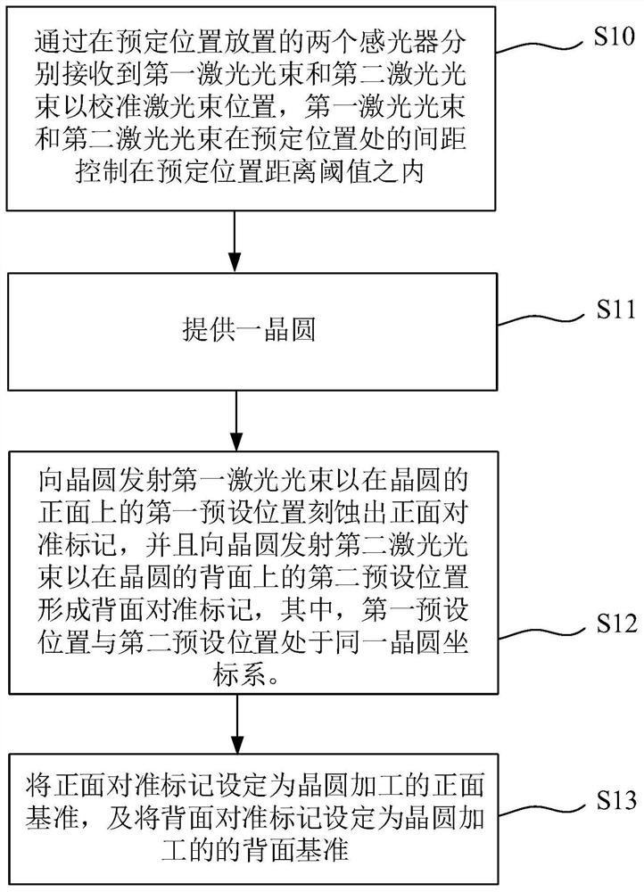
[0062] The invention provides a wafer crystal back alignment method. refer to figure 1 , the crystal back alignment method includes:
[0063] S11. Provide a wafer.
[0064] S12. Sending a first laser beam to the wafer to etch a front alignment mark at a first preset position on the front side of the wafer, and sending a second laser beam to the wafer to etch a second alignment mark on the back side of the wafer. The back alignment mark is etched at the preset position, wherein the first preset position and the second preset position are in the same wafer coordinate system. Among them, the front and back of the wafer use the same coordinate system, that is, the coordinates from left to right are the X-axis direction from the center of the wafer as the origin, and the Y-axis direction is upward from the notch (notch) of the wafer. The front (X, Y) coordinates are the back point coordinates.
[0065] S13 , setting the front alignment mark as a front reference for wafer proces...
Embodiment 2
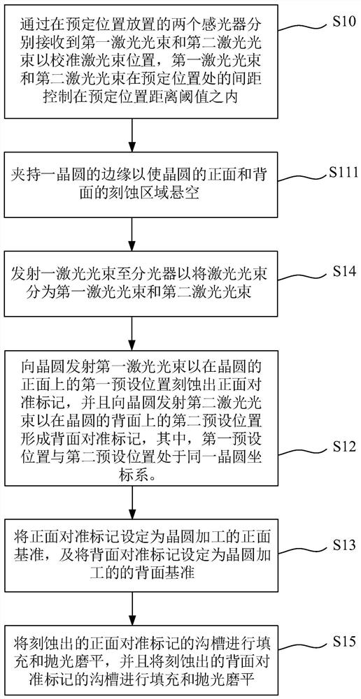
[0072] The crystal back alignment method of the wafer of this embodiment is a further improvement to Embodiment 1, specifically:
[0073] refer to figure 2 , step S11 specifically includes:
[0074] S111 , clamping the edge of a wafer to suspend the etching regions on the front and back of the wafer.
[0075] Before step S12, the crystal back alignment method also includes:
[0076] S14. Send a laser beam to the beam splitter to split the laser beam into a first laser beam and a second laser beam.
[0077] After step S13, the crystal back alignment method also includes:
[0078] S15 , filling and polishing the etched grooves of the front alignment marks, and filling and polishing the etched grooves of the back alignment marks.
[0079] The crystal back alignment method of the wafer in this embodiment uses the first laser beam and the second laser beam separated by the same laser beam to respectively etch the front alignment mark and the back alignment mark, and the front ...
Embodiment 3
[0081] This embodiment provides a wafer back alignment device. The crystal back alignment equipment implements the wafer back alignment method in Embodiment 1 or Embodiment 2.
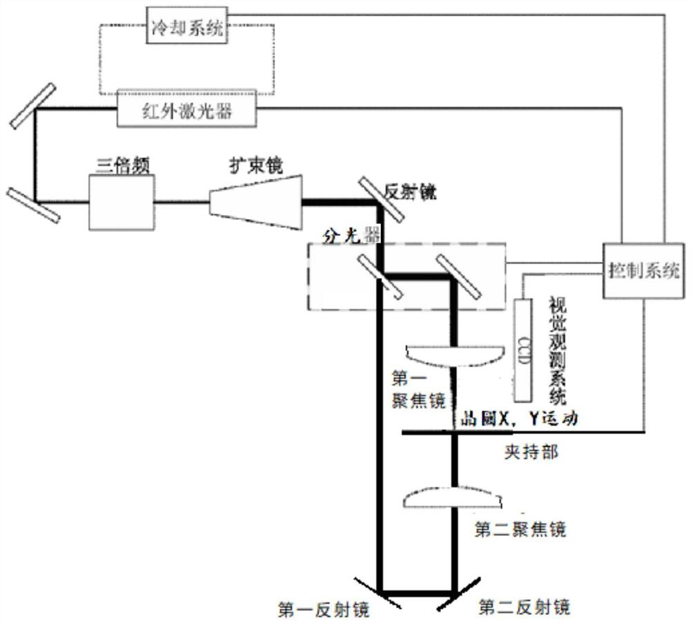
[0082] refer to image 3 and 4 , the crystal back alignment device includes: a controller 101 . The control system includes a controller 101 ( Figure 4 not shown).
[0083] The controller 101 is used to output control laser emission instructions to emit a first laser beam to the wafer to be aligned to etch a front alignment mark at a first preset position on the front surface of the wafer, and emit a first laser beam to the wafer. Two laser beams etch a back alignment mark at a second preset position on the back side of the wafer, wherein the first preset position and the second preset position are in the same wafer coordinate system, that is, the center of the wafer is The origin coordinates are the X-axis direction from left to right, and the Y-axis direction upward from the notch (notch) of th...
PUM
 Abstract
Description
Claims
Application Information
 - R&D
- Intellectual Property
- Life Sciences
- Materials
- Tech Scout
- Unparalleled Data Quality
- Higher Quality Content
- 60% Fewer Hallucinations
Browse by: Latest US Patents, China's latest patents, Technical Efficacy Thesaurus, Application Domain, Technology Topic, Popular Technical Reports.
© 2025 PatSnap. All rights reserved.Legal|Privacy policy|Modern Slavery Act Transparency Statement|Sitemap|About US| Contact US: help@patsnap.com