Method for optimizing access efficiency of DDR4 SDRAM in FPGA

An optimization method and access efficiency technology, applied in program control design, instrumentation, electrical digital data processing, etc., can solve problems such as reducing the access efficiency of DDR4 SDRAM, and achieve the effect of reducing the impact of access efficiency and improving access efficiency.

Pending Publication Date: 2021-06-25
无锡芯思维科技有限公司
View PDF0 Cites 0 Cited by
  • Summary
  • Abstract
  • Description
  • Claims
  • Application Information

AI Technical Summary

Problems solved by technology

[0004] However, user designs on many occasions require random access to DDR4 SDRAM. The access address is random, and it will inevitably switch the access row (Row) freq

Method used


Image

  • Method for optimizing access efficiency of DDR4 SDRAM in FPGA
  • Method for optimizing access efficiency of DDR4 SDRAM in FPGA
  • Method for optimizing access efficiency of DDR4 SDRAM in FPGA

Examples


Embodiment Construction

[0024] The present invention is described in further detail now in conjunction with accompanying drawing. These drawings are all simplified schematic diagrams, which only illustrate the basic structure of the present invention in a schematic manner, so they only show the configurations related to the present invention.

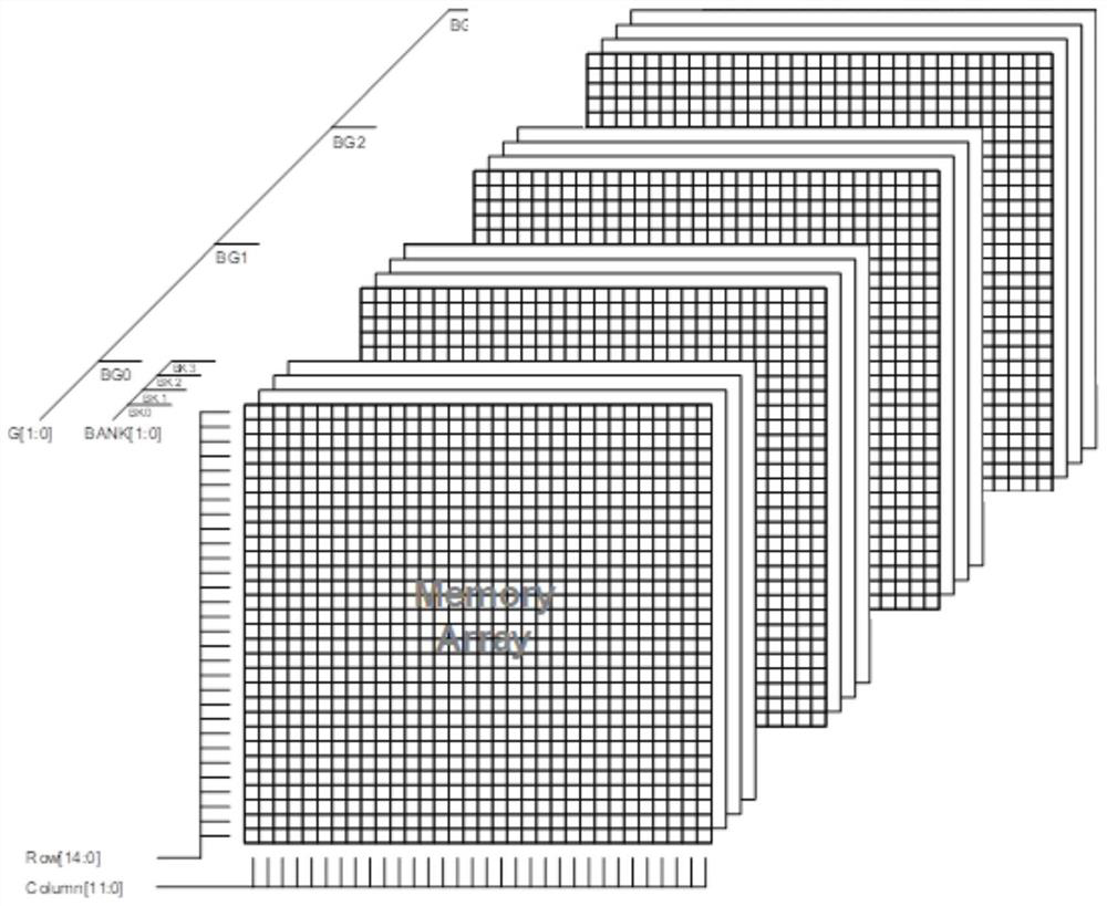
[0025] Such as figure 1 As shown, the internal storage structure of the DDR4 SDRAM chip is usually divided into several Bank groups, each Bank group has several Banks (usually 4-8 banks), each Bank has several row storage spaces, and each row There are several column storage spaces, so the storage address of DDR4 SDRAM is composed of BG (Bank group) address, Bank address, Row (row) address, and Column (column) address.

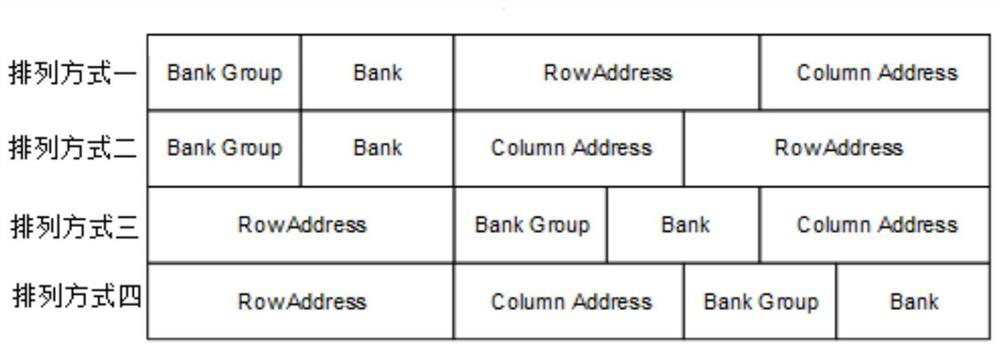
[0026] The arrangement of the access address of the access command for the user to access the memory space of DDR4 SDRAM can refer to figure 2 , figure 2 Although four arrangements are shown in , the addresses in each arrangement have BG ...


PUM


Abstract

The invention relates to a DDR4SDRAM access technology, and discloses a method for optimizing access efficiency of a DDR4 SDRAM in an FPGA. The method comprises the following steps that: S1, DDR4SDRAM access command of a user are input into a preprocessing module; S2, the preprocessing module sorts the input access commands according to sorting rules to form new command queues, then the new command queues are sequentially sent to the DDR4SDRAM, the preprocessing module is added in an FPGA system to sort the access commands of the user, the access commands with the same Row address in the same bank are classified into the same group, and then the pre-processing module sends access commands to the DDR4SDRAM group by group, so that only one activation action is needed when the DDR4SDRAM receives the access commands of the command group with the same Row address, and the operation of continuously opening and closing rows caused by continuously switching the Row address due to address randomness is saved.

Description

technical field [0001] The invention relates to the technical field of DDR4 SDRAM access, in particular to a DDR4 SDRAM access efficiency optimization method in FPGA. Background technique [0002] With the continuous development of semiconductor technology, FPGA chips have gradually been widely used in artificial intelligence, big data analysis, cloud computing, network communication, image processing, robotics, chip verification and many other fields, and are even replacing CPU and GPU in a few fields Or the position of DSP becomes the dominant chip. DDR4 SDRAM is the most widely used RAM-type dynamic random access memory in the current electronic system architecture, and it is also widely used in FPGA systems because of its large storage capacity and fast access speed. In addition to training the IO parameters of the DDR4 SDRAM chip and configuring the chip control registers and other initialization work after power-on, the access control of the DDR4 SDRAM chip also needs...

Claims


Application Information

Patent Timeline
IPC IPC(8): G06F13/16G06F9/38
CPCG06F13/1673G06F9/3856
Inventor 夏婷婷
Owner 无锡芯思维科技有限公司
Why Eureka
Try Eureka