Radiation-resistant fdsoi field effect transistor with sonos structure based on 22nm process and its preparation method

A field-effect transistor and anti-irradiation technology, which is applied in semiconductor/solid-state device manufacturing, semiconductor devices, electrical components, etc., can solve problems such as sub-threshold characteristic degradation, increased off-state leakage current, and reduced threshold voltage of FDSOI devices. , to achieve the effect of not easy to reverse type, less cost increase, and improved radiation resistance performance

Active Publication Date: 2022-07-22
XIDIAN UNIV
View PDF12 Cites 0 Cited by
  • Summary
  • Abstract
  • Description
  • Claims
  • Application Information

AI Technical Summary

Problems solved by technology

[0003] However, since there is no BOX structure as the device feature size shrinks, it is still sensitive to the total dose effect
Irradiation generates a large amount of trapped charges in the BOX layer, and then forms a leakage path at the lower interface of the channel, which leads to a decrease in the threshold voltage of the FDSOI device, an increase in the off-state leakage current, and degradation of subthreshold characteristics.

Method used


Image

  • Radiation-resistant fdsoi field effect transistor with sonos structure based on 22nm process and its preparation method
  • Radiation-resistant fdsoi field effect transistor with sonos structure based on 22nm process and its preparation method
  • Radiation-resistant fdsoi field effect transistor with sonos structure based on 22nm process and its preparation method

Examples


Embodiment 1

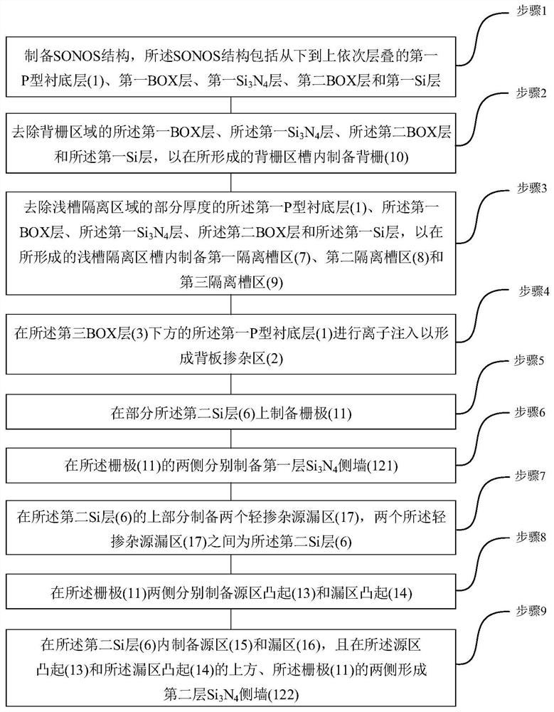
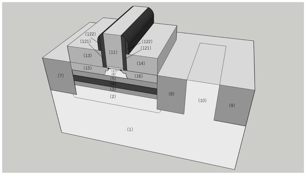
[0089] See figure 1 , figure 2 , figure 1 A schematic flowchart of a method for preparing a radiation-resistant FDSOI field effect transistor with a SONOS structure based on a 22nm process provided by an embodiment of the present invention; figure 2 A schematic structural diagram of a radiation-resistant FDSOI field effect transistor of a SONOS structure based on a 22nm process provided by an embodiment of the present invention. The invention provides a preparation method of a SONOS structure radiation-resistant FDSOI field effect transistor based on a 22nm process, the preparation method comprising the following steps:

[0090] Step 1. Prepare a SONOS structure. The SONOS structure includes a first P-type substrate layer 1, a first BOX layer, and a first Si layer that are sequentially stacked from bottom to top. 3 N 4 layer, the second BOX layer and the first Si layer.

[0091] Step 1.1, select the first P-type substrate layer 1;

[0092] Step 1.2, using a dry oxygen ...

Embodiment 2

[0176]The present embodiment provides a specific preparation method of a radiation-resistant FDSOI field effect transistor with a SONOS structure based on a 22nm process on the basis of the above-mentioned embodiments, and the preparation method includes the following steps:

[0177] Step 1. Make a SONOS structure.

[0178] 1.1) Thermally oxidize the first P-type substrate layer 1 to grow a thin SiO with a thickness of 10 nm by a dry oxygen process at a temperature of 1200 °C 2 layer, in SiO 2 10 nm thick Si deposited by atomic layer deposition 3 N 4 layer, then in Si 3 N 4 5nm thick SiO deposited on the layer 2 Floor;

[0179] 1.2) Use the standard 300mm SOI manufacturing process based on Smart Cut to oxidize the first silicon wafer with a thickness of 5nm and H+ ion implantation to prepare the second silicon wafer, and then hydrophilicize the first P-type substrate layer 1 and the second silicon wafer sexual bonding;

[0180] 1.3) In the ultra-high vacuum CVD reactio...

Embodiment 3

[0217] This embodiment provides a specific preparation method for a radiation-resistant FDSOI field effect transistor with a SONOS structure based on a 22nm process on the basis of the above-mentioned embodiments. 3 N 4 A 22nm FDSOI field effect transistor with a layer thickness of 10nm and a top layer BOX thickness of 15nm includes the following steps:

[0218] Step 1. Make a SONOS structure.

[0219] 1.1) Thermally oxidize the first P-type substrate layer 1 to grow a thin SiO with a thickness of 10 nm by a dry oxygen process at a temperature of 1250 °C 2 layer, in SiO 2 10 nm thick Si deposited by atomic layer deposition 3 N 4 layer, then in Si 3 N 4 5nm thick SiO deposited on the layer 2 Floor;

[0220] 1.2) Using the standard 300mm SOI manufacturing process based on Smart Cut, the first silicon wafer is oxidized with a thickness of 10nm and H+ ion implanted to prepare the second silicon wafer, and then the first P-type substrate layer 1 and the second silicon wafer a...


PUM

PropertyMeasurementUnit
thicknessaaaaaaaaaa
thicknessaaaaaaaaaa
thicknessaaaaaaaaaa

Abstract

The invention relates to a SONOS structure radiation-resistant FDSOI field effect transistor based on a 22nm process and a preparation method thereof. The method includes: making a SONOS structure, making a back gate, making a shallow trench isolation, making a back plate doping, making a high-K gate oxide and polysilicon gate, making the first layer of Si 3 N 4 Side walls, lightly doped source and drain, source and drain protrusions, source and drain regions, surface cleaning, and the device is completed. The present invention adds Si to the common BOX layer 3 N 4 layer, the BOX layer is divided into upper and lower layers, the introduced potential barrier increases the recombination of electrons and holes, and reduces the number of traps trapped in the BOX layer under the action of irradiation. 3 N 4 The trapped negative charges are generated in the layer, which offsets the effect of a part of the trapped positive charges in the BOX layer, so that the depth of the channel near the interface of the BOX layer is not easy to inversion, and the radiation resistance performance of the device is improved.

Description

technical field [0001] The invention belongs to the technical field of semiconductor devices, and relates to a SONOS structure anti-radiation FDSOI field effect transistor based on a 22nm process and a preparation method thereof. Background technique [0002] With the rapid development of the semiconductor industry, ordinary bulk silicon MOS (metal-oxide-semiconductor) devices can no longer meet the needs of the industry, and FDSOI (fully depleted silicon-on-insulator) devices are The leakage current has become an option to replace bulk silicon devices. FDSOI devices have significant advantages of high performance and low power consumption. The BOX layer (buried oxide layer) and the very thin top silicon layer can significantly reduce parasitic capacitance and junction leakage current. These excellent characteristics are important for semiconductor integrated circuits to continue to chase Moore's Law. significant. And because of its all-dielectric isolation structure, it h...

Claims


Application Information

Patent Timeline
Patent Type & Authority Patents(China)
IPC IPC(8): H01L21/336H01L29/06H01L29/10H01L29/78
CPCH01L29/66484H01L29/66492H01L29/7831H01L29/7833H01L29/0607H01L29/0684H01L29/1083
Inventor 刘红侠李战东余文龙王东郭丹
Owner XIDIAN UNIV
Why Eureka
Try Eureka