Cover plate, chip wafer packaging method and chip airtight packaging method

A technology of wafer packaging and packaging methods, which is applied in the fields of electrical components, semiconductor/solid-state device manufacturing, circuits, etc., can solve the problems of high cost and large volume of airtight packaging, and achieve the effect of low cost and small volume

Inactive Publication Date: 2021-06-25
北京万应科技有限公司
View PDF7 Cites 0 Cited by
  • Summary
  • Abstract
  • Description
  • Claims
  • Application Information

AI Technical Summary

Problems solved by technology

[0004] The purpose of the present invention is to overcome the disadvantages of large volume and high cost of hermetic packaging of chips in the prior art, and provide a cover plate, a chip wafer packaging method and a chip hermetic packaging method

Method used


Image

  • Cover plate, chip wafer packaging method and chip airtight packaging method
  • Cover plate, chip wafer packaging method and chip airtight packaging method
  • Cover plate, chip wafer packaging method and chip airtight packaging method

Examples


Embodiment 1

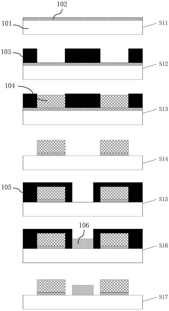
[0053] Such as figure 1 as shown, figure 1 It is a work flow chart of a cover wafer packaging method provided in Embodiment 1 of the present invention, including:

[0054] Step S11: making the first metal layer 102 on the front of the cover plate 101;

[0055] Step S12: making a first mask 103 on the first metal layer 102 to wrap the area to be sealed or the sensing area of ​​the chip;

[0056] Step S13: making a first circuit pattern 104 in the gap of the first mask 103;

[0057] Step S14: removing the first mask 103 and performing etching to obtain a cover wafer.

[0058] Specifically:

[0059] Step S11, electroless copper plating: electroplate a metal layer on the front of the cover plate 101 by electroless copper plating, sputtering or vapor deposition of metals such as Ti, TiW, Cr, Co, etc., to play the role of a barrier layer and an adhesion layer. The cover plate 101 The material can be silicon, glass, metal and other wafer materials;

[0060] Step S12, electropla...

Embodiment 2

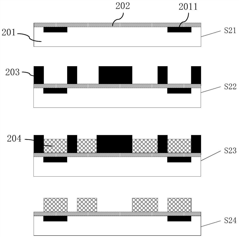
[0076] Such as figure 2 as shown, figure 2 It is a chip wafer packaging method provided in Embodiment 2 of the present invention, including:

[0077] Step S21: making a second metal layer 202 on the front side of the chip 201;

[0078] Step S22: making a third mask 203 at a position corresponding to the bonding pad 2011 of the chip 201 and the first circuit pattern of the cover wafer;

[0079] Step S23: making a third circuit pattern 204 within the gap of the third mask 203;

[0080] Step S24: removing the third mask 203 and performing etching to obtain a chip wafer.

[0081] Specifically:

[0082] Step S21, electroless copper plating: electroplating a metal layer on the front side of the chip 201 by electroless copper plating, sputtering or vapor deposition of metals such as Ti, TiW, Cr, Co, etc., to play the role of a barrier layer and an adhesion layer, and the chip 201 is completed Chips of application-specific integrated circuits or micro-electro-mechanical systems...

Embodiment 3

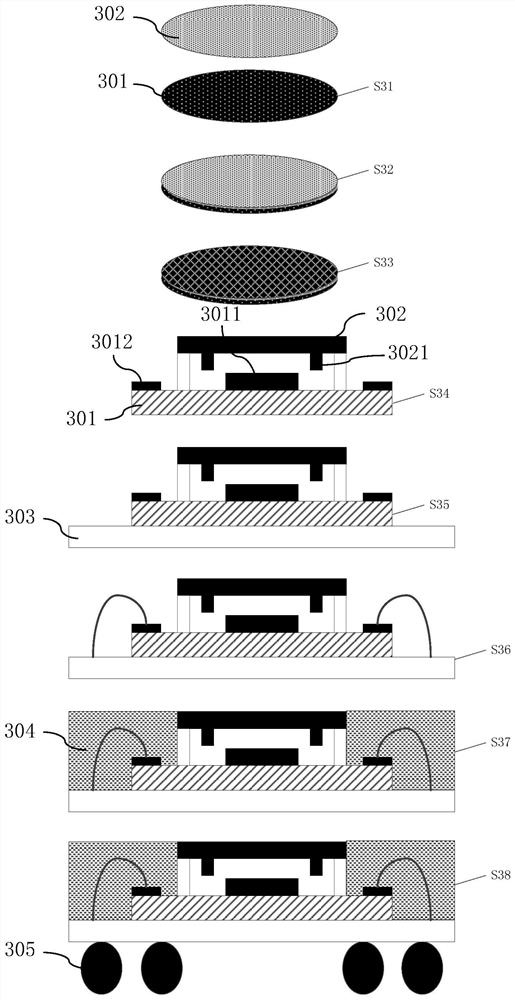
[0092] Such as image 3 as shown, image 3 It is a chip hermetic packaging method provided in Embodiment 3 of the present invention, including:

[0093] Step S31: use the aforementioned chip wafer packaging method to package the chip to obtain a chip wafer 301, and use the aforementioned cover wafer packaging method to package the cover to obtain a cover wafer 302;

[0094] Step S32: bonding the front surface of the cover wafer 302 and the front surface of the chip wafer 301 through the first metal layer and the second metal layer, so that the first circuit pattern of the cover wafer 302 wraps the chip wafer 301. Sealing area or sensing area 3011;

[0095] Step S33: Scribing the cover wafer 302 on the back side of the cover wafer 302, and exposing the bonding pads 3012 of the chip wafer 301;

[0096] Step S34: Scribing the chip wafer 301 at the position corresponding to the bonding pad 3012 of the chip wafer 301 to obtain a chip structure including the cover wafer 302 and t...


PUM


Abstract

The invention discloses a cover plate, a chip wafer packaging method and a chip airtight packaging method. The cover plate wafer packaging method comprises the steps that: a first metal layer is manufactured on the front face of the cover plate; a first mask for wrapping a to-be-sealed area or a sensing area of the chip is manufactured on the first metal layer; a first circuit pattern is manufactured in the gap of the first mask; and the first mask is removed, and etching is carried out to obtain a cover plate wafer. By means of the method, the cover plate wafer and the chip wafer are obtained by performing wafer-level packaging on the cover plate and the chip, and when airtight packaging is performed, airtight packaging is performed on the to-be-sealed area or the sensing area of the chip wafer through the cover plate wafer, so that airtight packaging of the chip is realized, the size of the chip is small, the application of the chip to portable products is facilitated, and the cost is low.

Description

technical field [0001] The invention relates to the technical field of electronic component packaging, in particular to a cover plate, a chip wafer packaging method and a chip hermetic packaging method. Background technique [0002] Many chip packages require high airtight, small package form. Traditional hermetic packages include metal package and ceramic package, which are bulky, thick, costly and complicated. The main features of the metal package and the ceramic package are as follows: place the die (Die) inside the metal package or the ceramic package, and wire it to the pad (Pad) inside the package through the wire (Wirebond) , A sealing cover is set on the tube shell to isolate the external atmospheric environment. [0003] However, due to the large volume of the existing metal package or ceramic package, the packaged chip structure is relatively thick, generally more than 2 mm in thickness, which is not conducive to application in some portable products. , because...

Claims


Application Information

Patent Timeline
Patent Type & Authority Applications(China)
IPC IPC(8): H01L21/50H01L21/56
CPCH01L21/50H01L21/56
Inventor 黄玲玲
Owner 北京万应科技有限公司
Why Eureka
Try Eureka