Cover plate structure, chip structure and airtight chip structure

A chip structure and airtight technology, applied in the direction of electrical components, electric solid devices, circuits, etc., can solve the problems of large volume and high cost of airtight packaging, and achieve the effect of small size and low cost

Pending Publication Date: 2021-06-25
北京万应科技有限公司
View PDF0 Cites 0 Cited by
  • Summary
  • Abstract
  • Description
  • Claims
  • Application Information

AI Technical Summary

Problems solved by technology

[0004] The purpose of the present invention is to overcome the disadvantages of large volume and high cost of the hermetic packaging of chips in the prior art, and provide a cover plate structure, a chip structure and an airtight chip structure

Method used


Image

  • Cover plate structure, chip structure and airtight chip structure
  • Cover plate structure, chip structure and airtight chip structure
  • Cover plate structure, chip structure and airtight chip structure

Examples


Embodiment 1

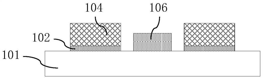
[0030] Such as figure 1 as shown, figure 1 It is a cover plate structure provided by Embodiment 1 of the present invention, including a cover plate disc 101, a first metal layer 102 is provided on the front side of the cover plate disc 101, and a The first circuit patterns 104 are electrically connected to obtain a cover wafer.

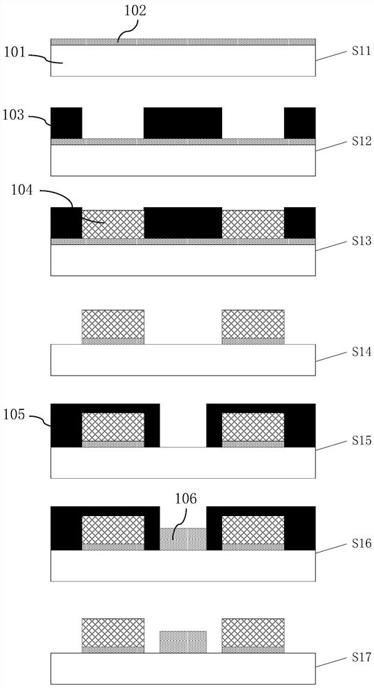
[0031] Specifically, such as figure 2 As shown, the cover plate structure is packaged by the following steps:

[0032] Step S11, making the first metal layer 102 on the front side of the cover plate 101: Electroplating the first metal layer 102 on the front side of the cover plate 101 by electroless copper plating, sputtering or vapor deposition of Ti, TiW, Cr, Co, etc. barrier layer and adhesion layer, the material of the cover plate 101 can be silicon, glass, metal and other wafer materials;

[0033] Step S12, making a first mask 103 on the first metal layer 102 that wraps the area to be sealed or the sensing area of ​​the chip: electroplating ...

Embodiment 2

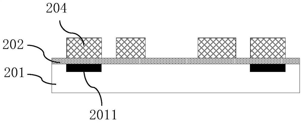
[0045] Such as image 3 as shown, image 3It is a chip structure provided by Embodiment 2 of the present invention, including a chip 201, a second metal layer 202 is provided on the front side of the chip 201, and a second metal layer 202 is provided at a position corresponding to the bonding pad 2011 of the chip 202 and the first circuit pattern of the cover wafer. There is a third circuit pattern 204 electrically connected to the second metal layer 202, resulting in a chip wafer.

[0046] Specifically, as Figure 4 As shown, the chip structure is packaged by the following steps:

[0047] Step S21, making the second metal layer 202 on the front of the chip 201: electroplating the second metal layer 202 on the front of the chip 201 by electroless copper plating, sputtering or vapor deposition of metals such as Ti, TiW, Cr, Co, etc., to act as a barrier layer and the adhesion layer, the chip 201 is a chip that completes processes such as application-specific integrated circu...

Embodiment 3

[0055] Such as Figure 5 as shown, Figure 5 It is a structural schematic diagram of an airtight chip structure provided by Embodiment 3 of the present invention, including the aforementioned cover structure, the aforementioned chip structure, and the substrate 303, and the cover wafer 302 of the cover structure The front surface of the chip wafer 301 of the chip structure is electrically connected through the first metal layer and the second metal layer, so that the first circuit pattern of the cover wafer 302 wraps the area to be sealed or the sensing area 3011 of the chip wafer 301 , the back of the chip wafer 301 is attached to the front of the substrate 303, and the substrate 303 is electrically connected to the pad 3012 of the chip wafer 301, and the cover wafer 302, the chip wafer 301 and the substrate 303 are embedded in the organic resin 304 Inside.

[0056] Specifically, as Figure 6 As shown, the hermetic chip structure is packaged by the following steps:

[005...


PUM


Abstract

The invention discloses a cover plate structure, a chip structure and an airtight chip structure. The cover plate structure comprises a cover plate wafer; the front surface of the cover plate wafer is provided with a first metal layer; the first metal layer is provided with a first circuit pattern electrically connected with the first metal layer; and therefore, a cover plate wafer is obtained. By means of the method, the cover plate wafer and the chip wafer are obtained by performing wafer-level packaging on the cover plate and the chip; and when airtight packaging is performed, airtight packaging is performed on the to-be-sealed area or the sensing area of the chip wafer through the cover plate wafer, so that airtight packaging of the chip is realized, the size of the chip is small, the application of the chip to portable products is facilitated, and the cost is low.

Description

technical field [0001] The invention relates to the technical field of electronic chip packaging, in particular to a cover plate structure, a chip structure and an airtight chip structure. Background technique [0002] Many chip packages require high airtight, small package form. Traditional hermetic packages include metal package and ceramic package, which are bulky, thick, costly and complicated. The main features of the metal package and the ceramic package are as follows: place the die (Die) inside the metal package or the ceramic package, and wire it to the pad (Pad) inside the package through the wire (Wirebond) , A sealing cover is set on the tube shell to isolate the external atmospheric environment. [0003] However, due to the large volume of the existing metal package or ceramic package, the packaged chip structure is relatively thick, generally more than 2 mm in thickness, which is not conducive to application in some portable products. , because the cost of t...

Claims


Application Information

Patent Timeline
Patent Type & Authority Applications(China)
IPC IPC(8): H01L23/04H01L23/10H01L23/488
CPCH01L23/04H01L23/10H01L23/488
Inventor 黄玲玲
Owner 北京万应科技有限公司
Why Eureka
Try Eureka