MEMS device airtightness packaging method

An encapsulation method and air tightness technology, applied in the field of MEMS processing, can solve the problems of vacuum degree limitation, difficult control, device damage, etc., and achieve the effect of small internal stress and large bonding strength

Inactive Publication Date: 2008-08-06
PEKING UNIV
View PDF0 Cites 6 Cited by
  • Summary
  • Abstract
  • Description
  • Claims
  • Application Information

AI Technical Summary

Problems solved by technology

Thin film sealing technology uses sacrificial layer method to etch out the cavity structure, through the small holes on the cavity and the vacuum environment when depositing the film, the cavity has a certain degree of vacuum, and the film is selectively deposited on the small hole seal to complete the gas Hermetic packaging, but the corros

Method used


Image

  • MEMS device airtightness packaging method
  • MEMS device airtightness packaging method
  • MEMS device airtightness packaging method

Examples


Embodiment Construction

[0035] The following specific examples help to understand the characteristics and advantages of the present invention, but the implementation of the present invention is by no means limited to the described examples.

[0036] A specific embodiment of the hermetic packaging method of the present invention includes as Figure 6 to Figure 12 Process steps shown:

[0037] 1. Preparation of the chamber and pre-preparation of the top cover

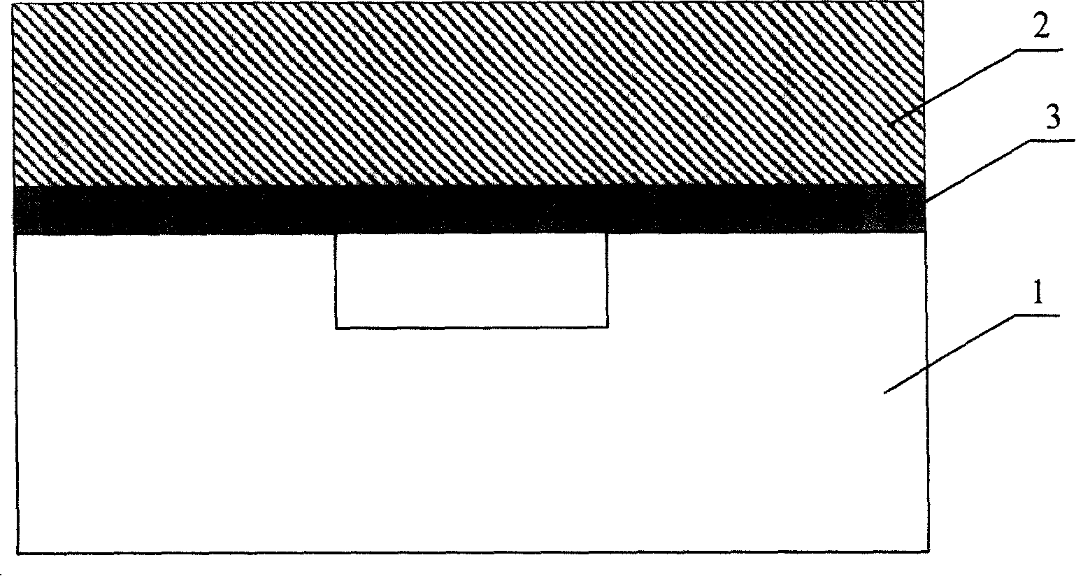
[0038] see Image 6 , the material of substrate A for processing cavity grooves is glass, and the designed cavity is etched with HF through the mask plate. The substrate B used as the top cover is a silicon wafer. First, a silicon dioxide layer 5 and a silicon nitride layer 6 are thermally grown on the silicon wafer, and then photoetched on the silicon nitride according to the size and shape of the groove on the substrate A. Etching defines the pattern of the silicon nitride film.

[0039] When the photoresist outside the silicon cap is remo...


PUM


Abstract

The invention provides an air tightness encapsulation method for a widely applied MEMS device, which is a bonding technology based on an interlayer and realized by matching with air tightness materials such as coated metal and so on. The interlayer material refers to adhesive organic matters such as photoresist and so on; under low temperature and low pressure, high bonding strength and extremely small internal stress can be realized; at the same time, bonding mode requires less for an upper surface and a lower surface; even if the surface is not smooth, the bonding can be successfully conducted; after the air tightness materials are coated, the leakage rate is less than 1 multiplies 10<-8>cm<3>/s, which completely meets the requirement of practical application.

Description

technical field [0001] The invention belongs to the technical field of micro-electro-mechanical systems (MEMS), and in particular relates to an airtight packaging method based on interlayer bonding. Background technique [0002] At present, many MEMS devices have been developed, but in the actual application process, packaging technology has always been one of the key technologies that plague the development and practical application of MEMS devices, and hermetic packaging is especially difficult. Due to the complexity of MEMS devices, the cost of MEMS packaging accounts for 70% to 90% of MEMS products. Packaging is a very important part of MEMS device design. On a silicon wafer, the size of MEMS devices can range from 1μm to more than 1mm. During storage and work, external temperature, humidity, mechanical vibration, acceleration, dust particles, and other physical damage, and even radiation will have unpredictable effects on the work of the device. However, most MEMS de...

Claims


Application Information

Patent Timeline
IPC IPC(8): B81C3/00
Inventor 陈兢吴烨娴赵刚
Owner PEKING UNIV
Why Eureka
Try Eureka