Chip packaging structure and preparation method thereof

A chip packaging structure and chip technology, which is applied in semiconductor/solid-state device manufacturing, semiconductor/solid-state device parts, semiconductor devices, etc., can solve the problems of reducing chip quality, chip failure, wire bonding, etc., to solve chip failure, The effect of expanding the scope of action and improving efficiency

Pending Publication Date: 2022-05-06
GUILIN UNIV OF ELECTRONIC TECH
View PDF0 Cites 0 Cited by
  • Summary
  • Abstract
  • Description
  • Claims
  • Application Information

AI Technical Summary

Problems solved by technology

[0004] The purpose of the present invention is to provide a chip packaging structure and its preparation method, which can solve the problem of delamination and cracking of some devices absorbed by water vapor in the current injection molding packaging, and lead bonding is easily caused during injection molding, which reduces the quality of the chip and even causes the chip to fail.

Method used


Image

  • Chip packaging structure and preparation method thereof
  • Chip packaging structure and preparation method thereof
  • Chip packaging structure and preparation method thereof

Examples


Embodiment 1

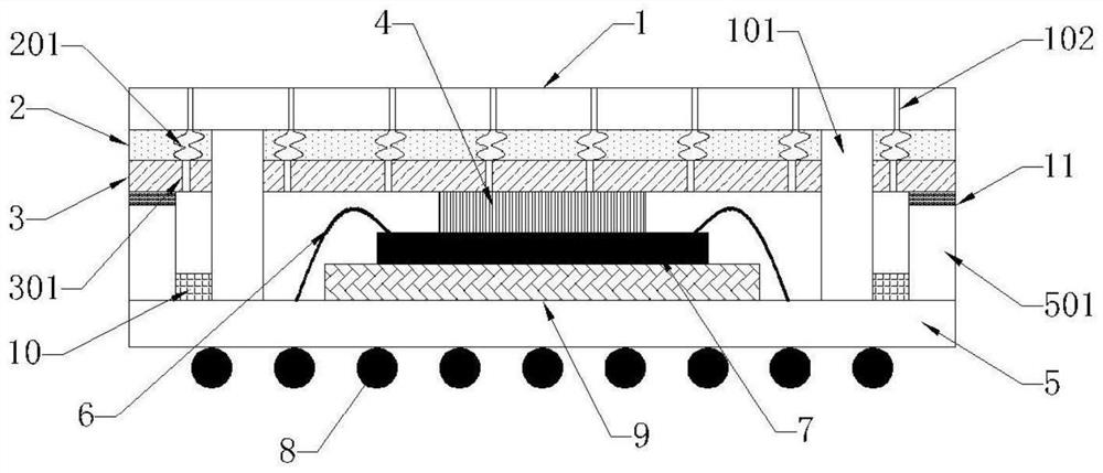
[0042] Such as Figure 1-7 As shown, a chip packaging structure is characterized in that it includes a cover plate and a base. The cover plate includes a cover plate base disc 1, a heat dissipation layer 2, and a moisture absorption layer 3 that are superimposed and fixedly connected layer by layer. 101, the cover plate retaining member 101 runs through the heat dissipation layer 2 and the moisture absorption layer 3 and extends out of the moisture absorption layer 3 for a predetermined distance, as a fitting part connecting the cover plate to the base; Several micro-holes 102 are opened at a distance, and several micro-fluidic channels 201 are opened corresponding to the micro-holes 102 in the heat dissipation layer 2. The micro-fluidic channels 201 communicate with the micro-holes 102, and several water-absorbing holes 301 are set on the moisture-absorbing layer 3. , the water absorption hole 301 has a Nepenthes structure, and the water absorption hole 301 communicates with...

Embodiment 2

[0055] Such as Figure 8-11 Shown, a kind of preparation method of chip packaging structure comprises the following steps:

[0056] S1: Using a ceramic, metal or glass wafer to prepare the cover plate substrate wafer 1, and making micro holes 102 on the cover plate base through the laser etching process or plasma etching process in the micro-nano processing technology;

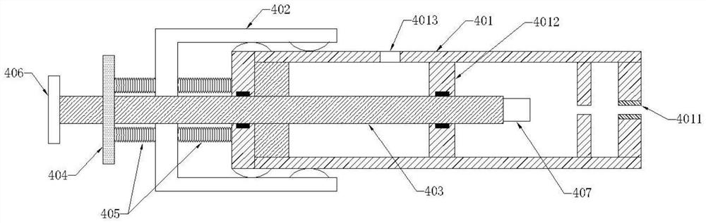
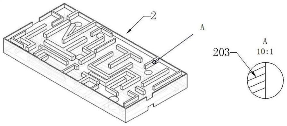
[0057] S2: Use a metal or ceramic wafer to prepare the heat dissipation layer 2, make a mask on the heat dissipation layer material by coating photoresist, exposure, development and other processes, and use the laser etching process to manufacture the microfluidic channel 201, through rapid etching The process etches away the substrate other than the pattern of the microfluidic channel 201, removes the mask, and obtains the heat dissipation layer 2, and manufactures the gourd-shaped through hole 202 through the laser etching hole technology in the micro-nano processing technology, which is used to connect the ...


PUM

PropertyMeasurementUnit
thicknessaaaaaaaaaa
pore sizeaaaaaaaaaa
thicknessaaaaaaaaaa

Abstract

The invention discloses a chip packaging structure and a packaging method thereof.The packaging structure comprises a cover plate and a base, the cover plate comprises a cover plate substrate wafer, a heat dissipation layer and a moisture absorption layer which are stacked layer by layer, a plurality of micro-holes are evenly formed in the cover plate substrate wafer at preset intervals, a plurality of micro-fluidic channels are formed in the heat dissipation layer and correspond to the micro-holes, and the moisture absorption layer is arranged on the base. The moisture absorption layer is provided with a plurality of water absorption holes, and the water absorption holes are communicated with the microfluidic channels; the base comprises a base substrate wafer, the chip is installed in the middle of the upper portion of the base substrate wafer and electrically connected with the base substrate wafer through a bonding wire, and BGA ball mounting is carried out on the lower portion of the base substrate wafer to serve as a port for connecting the chip with the outside. The cover plate and the base are connected through parallel welding seams after being clamped. According to the invention, the problems of layering and cracking due to water vapor absorption of part of devices in current injection molding packaging and easy lead bonding, chip quality reduction and even chip failure during injection molding are solved.

Description

technical field [0001] The invention belongs to the technical field of chip packaging, and in particular relates to a chip packaging structure and a preparation method thereof. Background technique [0002] At present, the main processing method used for civilian chip packaging is injection molding. The material is heated and melted and then injected into the mold. During the injection molding process, thermal shock will inevitably occur on the wire bonding points and the frame. At the same time, thermal expansion may cause the package on the chip to squeeze the chip during subsequent use, causing the chip to break; moisture absorption may cause delamination and cracking during subsequent processing. Therefore, people began to improve the quality of chip packaging from the aspect of damp heat. [0003] For the moisture problem, people establish a hygroscopic level during storage and dry it before use. However, some devices will still absorb water vapor after drying and befo...

Claims


Application Information

Patent Timeline
Patent Type & Authority Applications(China)
IPC IPC(8): H01L23/04H01L23/26H01L23/10H01L23/367H01L23/473H01L21/50H01L21/52
CPCH01L23/04H01L23/26H01L23/10H01L23/367H01L23/473H01L21/50H01L21/52
Inventor 黄兆岭可帅李思远潘开林李春泉杨道国
Owner GUILIN UNIV OF ELECTRONIC TECH
Why Eureka
Try Eureka