Three-dimensional integrated airtight packaging interconnection structure and manufacturing method thereof

A technology of interconnect structure and manufacturing method, applied in the direction of electrical components, semiconductor/solid-state device manufacturing, electric solid-state devices, etc., can solve the problem that silicon-based packaging technology does not have air-tightness capability, silicon-based packaging technology is not air-tight, etc. problem, to achieve the effect of low cost, small size and high package integration

Pending Publication Date: 2022-03-08
NAT CENT FOR ADVANCED PACKAGING +1
View PDF0 Cites 1 Cited by
  • Summary
  • Abstract
  • Description
  • Claims
  • Application Information

AI Technical Summary

Problems solved by technology

[0004] The purpose of the present invention is to provide a three-dimensional integrated hermetic packaging interconnection structure and its manufacturing method to solve the problem that the existing common silicon-based packaging technology does not have the ability of airtightness
[0005] The purpose of the present invention is also to overcome the problem of non-airtightness of the existing silicon-based packaging process, and provide a three-dimensional integrated structure and manufacturing method of an airtight silicon-based cavity, which is used for the airtight integration of radio frequency heterogeneous chip microsystems

Method used


Image

  • Three-dimensional integrated airtight packaging interconnection structure and manufacturing method thereof
  • Three-dimensional integrated airtight packaging interconnection structure and manufacturing method thereof
  • Three-dimensional integrated airtight packaging interconnection structure and manufacturing method thereof

Examples


Embodiment Construction

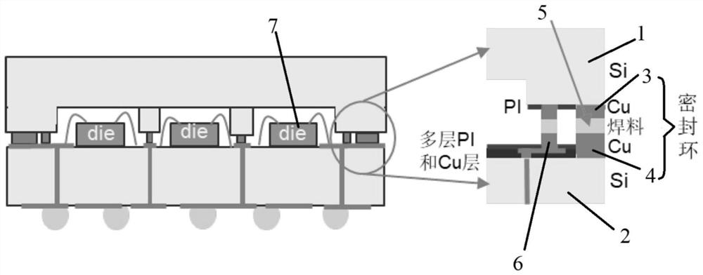
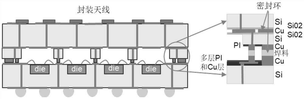
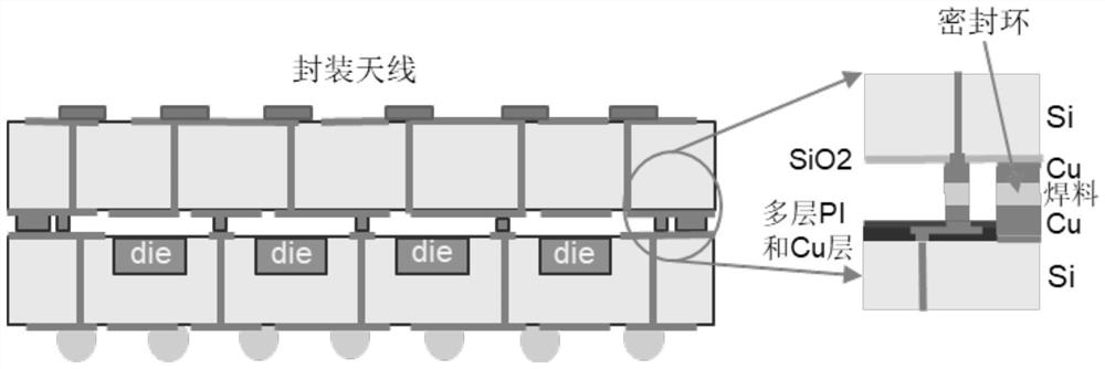
[0048] The present invention is further described below with reference to the accompanying drawings in conjunction with specific embodiments.

[0049] It should be noted that various components in the various figures may be shown exaggerated for illustration purposes and not necessarily to correct scale. In the various figures, identical or functionally identical components are provided with the same reference numerals.

[0050] In the present invention, unless otherwise specified, "arranged on," "arranged over," and "arranged over" do not exclude the case where there is an intermediate between the two. In addition, "arranged on or above" only means the relative positional relationship between two components, and in certain circumstances, such as after reversing the product direction, it can also be converted to "arranged under or below", and vice versa Of course.

[0051] In the present invention, each embodiment is only intended to illustrate the solution of the present in...


PUM


Abstract

The invention provides a three-dimensional integrated airtight packaging interconnection structure and a manufacturing method thereof, and the structure comprises an airtight silicon cavity upper cover which is configured to be capable of being connected with a first part of a sealing bonding ring; the airtight bottom silicon substrate is configured to be connected with the second part of the sealing bonding ring; and the sealing bonding ring is provided with an annular first part and an annular second part, and the first part and the second part are configured to be capable of forming an airtight silicon-based cavity between the airtight silicon cavity upper cover and the airtight bottom silicon substrate under the condition that the first part and the second part are jointed with each other.

Description

technical field [0001] The invention relates to the technical field of integrated circuits, in particular to a three-dimensional integrated air-tight packaging interconnection structure and a manufacturing method thereof. Background technique [0002] Radio frequency microsystem is the main means to achieve the goals of miniaturization, high density, wide operating frequency band, high work efficiency and high reliability of military and civil electronic systems such as new generation radar, electronic warfare and communication. With the rapid development of microwave / millimeter-wave circuit technology and advanced packaging technology, silicon-based 3D integration technology has become a popular choice for realizing light, miniaturized, high-efficiency RF microsystems due to its advantages of heterogeneous integration, light weight of substrates, and good thermal conductivity. It is an important technical means of density integration, and is a research hotspot at home and a...

Claims


Application Information

Patent Timeline
Patent Type & Authority Applications(China)
IPC IPC(8): H01L23/04H01L23/10H01L23/48H01L21/50H01L21/52
CPCH01L23/04H01L23/10H01L23/481H01L21/50H01L21/52H01L2224/48091H01L2924/15153H01L2924/00014
Inventor 李君戴风伟张凯
Owner NAT CENT FOR ADVANCED PACKAGING
Why Eureka
Try Eureka