Manufacturing method of display panel and display panel

A display panel and manufacturing method technology, applied in the direction of diodes, semiconductor devices, electrical components, etc., can solve problems such as cumbersome technical processes, achieve the effects of reducing cumbersomeness, improving production efficiency, and reducing the number of etching times

Pending Publication Date: 2021-06-29
KUNSHAN GO VISIONOX OPTO ELECTRONICS CO LTD
View PDF3 Cites 0 Cited by
  • Summary
  • Abstract
  • Description
  • Claims
  • Application Information

AI Technical Summary

Problems solved by technology

[0003] For display panels with blind holes, it is necessary to remove the inorganic layer in the hole area to improve the photographing effect of the camera in the hole area. However, in the prior art, multiple masks and etching processes are required to form blind holes in the production process of the display panel. The process is more cumbersome

Method used


Image

  • Manufacturing method of display panel and display panel
  • Manufacturing method of display panel and display panel
  • Manufacturing method of display panel and display panel

Examples


Embodiment Construction

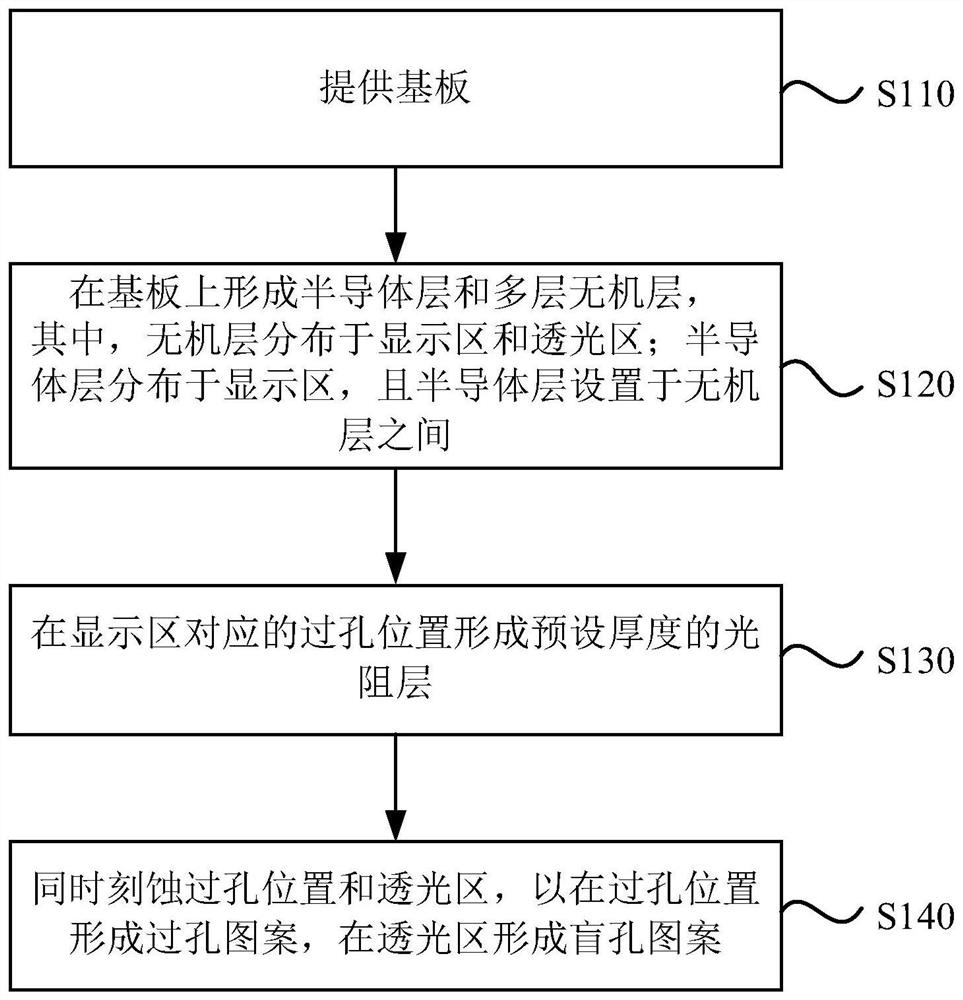
[0037] The present invention will be further described in detail below in conjunction with the accompanying drawings and embodiments. It should be understood that the specific embodiments described here are only used to explain the present invention, but not to limit the present invention. In addition, it should be noted that, for the convenience of description, only some structures related to the present invention are shown in the drawings but not all structures.

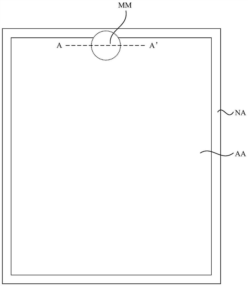
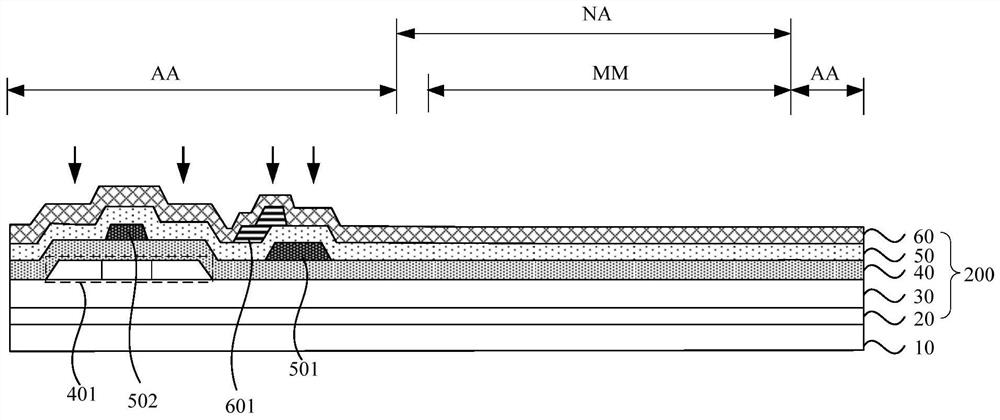
[0038] As mentioned in the background technology, in the manufacturing process of the array substrate of the existing display panel, it is necessary to etch the inorganic layer corresponding to the light-transmitting area to form a blind hole, and it is necessary to form an inorganic layer via hole in the display area of ​​the display panel for pixel Construction of the drive circuit. However, due to the large difference between the etching thickness of the inorganic layer corresponding to the light-transmitting a...


PUM

PropertyMeasurementUnit
Thicknessaaaaaaaaaa
Thicknessaaaaaaaaaa
Thicknessaaaaaaaaaa

Abstract

The embodiment of the invention discloses a manufacturing method of a display panel and the display panel. The manufacturing method of the display panel comprises the steps that a substrate is provided; a semiconductor layer and a plurality of inorganic layers are formed on the substrate, and the inorganic layers are distributed in a display area and a light-transmitting area; the semiconductor layer is distributed in the display area and is arranged between the inorganic layers; a photoresist layer with a preset thickness is formed at the position of the via hole corresponding to the display area; and the via hole position and the light-transmitting area are etched at the same time so as to form a via hole pattern at the via hole position and form a blind hole pattern in the light-transmitting area. Compared with the prior art, the technical scheme provided by the embodiment of the invention can simultaneously etch the via hole position and the light-transmitting area through one etching process to respectively form the via hole pattern and the blind hole pattern so that the etching times when the hole areas are formed at different positions can be reduced in the manufacturing process of the display panel, the complexity of the etching process is reduced, and the manufacturing efficiency of the display panel is improved.

Description

technical field [0001] Embodiments of the present invention relate to the field of display technology, and in particular, to a method for manufacturing a display panel and the display panel. Background technique [0002] Active matrix organic light emitting diode (Active Matrix Organic Light Emitting Diodes, AMOLED) display panel has become a mainstream product in the current display field due to its advantages of thinness, flexibility, and high luminous energy efficiency. [0003] For display panels with blind holes, it is necessary to remove the inorganic layer in the hole area to improve the photographing effect of the camera in the hole area. However, in the prior art, multiple masks and etching processes are required to form blind holes in the production process of the display panel. The process is more complicated. Contents of the invention [0004] Embodiments of the present invention provide a method for manufacturing a display panel and the display panel, so as t...

Claims


Application Information

Patent Timeline
IPC IPC(8): H01L27/32
CPCH10K59/65H10K59/12H10K59/1201
Inventor 金玉陆蕴雷王恩来马明冬张鹏辉黄佳兵
Owner KUNSHAN GO VISIONOX OPTO ELECTRONICS CO LTD
Why Eureka
Try Eureka