
Driving backboard and manufacturing method thereof, transfer method thereof and display device

A technology for driving backplanes and substrate substrates, applied in semiconductor/solid-state device manufacturing, electrical components, electrical solid-state devices, etc., can solve the problem of low transfer efficiency and product yield, high cost, and difficulty in realizing large-scale display panel production, etc. problem, to achieve the effect of improving production efficiency and product yield, meeting low cost, and preventing short circuit

Pending Publication Date: 2021-06-29
BOE TECH GRP CO LTD
View PDF9 Cites 0 Cited by
  • Summary
  • Abstract
  • Description
  • Claims
  • Application Information

AI Technical Summary

Problems solved by technology

However, when using related technologies to bond micro-LED chips, there are generally problems of high cost, low transfer efficiency and low product yield, and it is also difficult to realize the production of large-size display panels.

Method used


Image

  • Driving backboard and manufacturing method thereof, transfer method thereof and display device
  • Driving backboard and manufacturing method thereof, transfer method thereof and display device
  • Driving backboard and manufacturing method thereof, transfer method thereof and display device

Examples


Embodiment Construction

[0028] In order to make the purpose, technical solutions and advantages of the present disclosure clearer, the present disclosure will be further described in detail below in conjunction with specific embodiments and with reference to the accompanying drawings.

[0029] It should be noted that, unless otherwise defined, the technical terms or scientific terms used in the embodiments of the present disclosure shall have ordinary meanings understood by those skilled in the art to which the present disclosure belongs. "First", "second" and similar words used in the embodiments of the present disclosure do not indicate any sequence, quantity or importance, but are only used to distinguish different components. "Comprising" or "comprising" and similar words mean that the elements or items appearing before the word include the elements or items listed after the word and their equivalents, without excluding other elements or items. Words such as "connected" or "connected" are not lim...


PUM

PropertyMeasurementUnit
Thicknessaaaaaaaaaa
Diameteraaaaaaaaaa
Diameteraaaaaaaaaa

Abstract

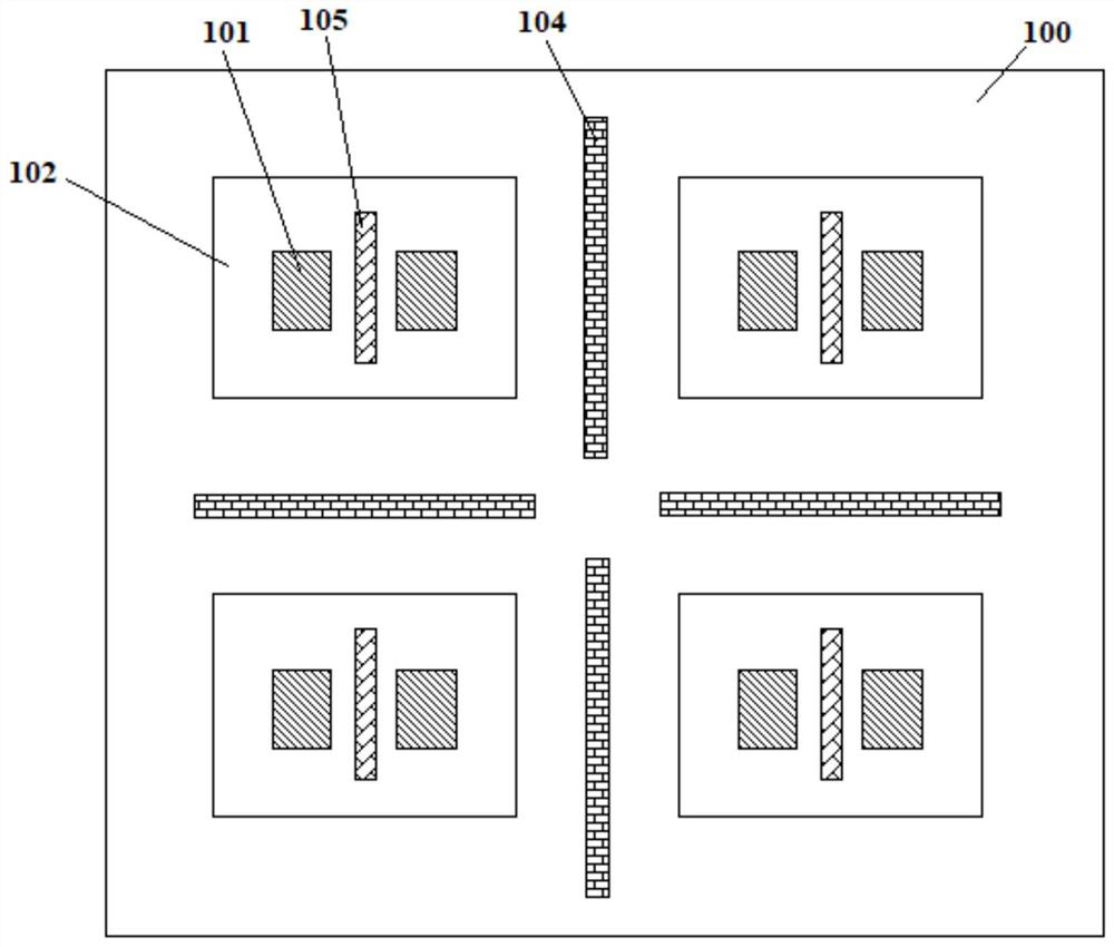
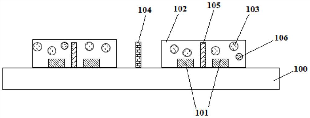
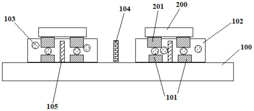
The invention provides a driving backboard, a manufacturing method thereof, a transfer method and a display device. The driving backboard comprises a substrate base plate, wherein the substrate comprises a plurality of pixel regions which are arranged in an array; a first retaining wall made of an insulating material is arranged between any two adjacent pixel regions; a pair of binding bonding pads is arranged in each pixel region, and a second retaining wall made of an insulating material is arranged between the binding bonding pads; each pixel region is further provided with a frame adhesive which is made of an insulating material and is doped with conductive microspheres; the frame glue is used for fixedly connecting the micro light-emitting diode chip to the corresponding pixel region and packaging the binding bonding pad and the second retaining wall in the pixel region; and the conductive microspheres are used for electrically connecting the electrodes of the micro light-emitting diode chips with the binding pads. According to the driving backboard, the requirements of low-cost and large-size display panel manufacturing can be met, and the manufacturing efficiency and the product yield can be effectively improved.

Description

technical field [0001] The present disclosure relates to the field of display technology, and in particular to a driving backplane, a manufacturing method thereof, a transfer method, and a display device. Background technique [0002] Compared with traditional liquid crystal display panels, Micro-LED display panels have the advantages of higher resolution, better contrast, faster response time and lower energy consumption, and have good application prospects, so they are regarded as For the next generation of display technology. [0003] In related technologies, micro-LED chips can only be prepared by epitaxial growth on a wafer substrate, and then tens of thousands to hundreds of thousands of micro-LED chips are transferred to a target substrate through a transfer substrate to form an LED array. During the transfer process of the micro-LED chip, it is necessary to bond the electrodes of the micro-LED chip to the bonding pads on the target substrate. However, when using re...

Claims


Application Information

Patent Timeline
IPC IPC(8): H01L33/48H01L33/62H01L27/15H01L21/683H01L21/67
CPCH01L33/486H01L33/62H01L21/67132H01L21/6835H01L27/156H01L2933/0033H01L2933/0066H01L2221/68322
Inventor 李树磊康昭谷新张笑黄华王明星赵梦华
Owner BOE TECH GRP CO LTD
Learn More