SMD (Surface Mount Device) quartz crystal resonator base and processing method thereof
A technology of quartz crystals and resonators, which is applied in the direction of electrical components and impedance networks, can solve the problems of difficult processing and high cost of multilayer ceramic boards, and achieve the effect of reducing material costs, meeting low costs, and broad application prospects
- Summary
- Abstract
- Description
- Claims
- Application Information
AI Technical Summary
Problems solved by technology
Method used
Image
Examples
Embodiment 1
[0038] The SMD quartz crystal resonator base of this implementation adopts a single-layer ceramic substrate,
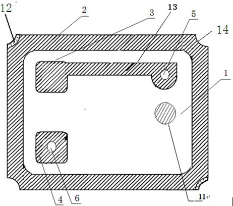
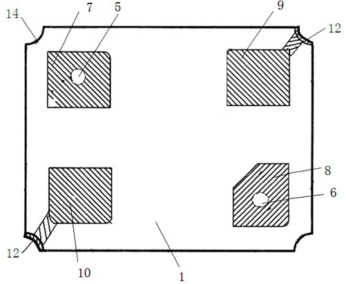
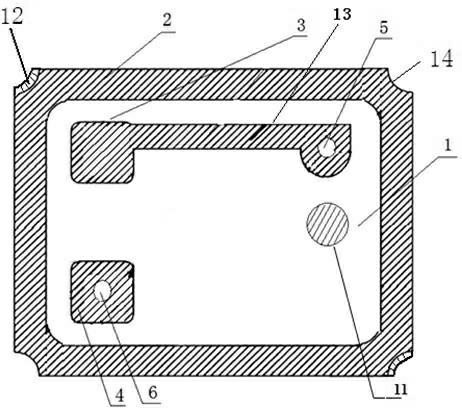
[0039] The four arc angles 14 of the single-layer ceramic substrate 1 are all designed as concave arc angles. The ceramic substrate 1 is opened with two first through holes 5 and second through holes 6 for pouring conductive materials. The ceramic substrate 1 Do metallization for electrode connection;
[0040] The upper surface of the ceramic substrate 1 is distributed with: a metal ring platform 2 sintered on the metal coating on the outer periphery of the upper surface, and a pair of first metal support platform 3 and second metal support platform 4 for wafer dispensing on the left side of the ring. , the right side of the ring is provided with a third metal support platform 11 for supporting the wafer;
[0041] The lower surface of the ceramic substrate 1 is distributed with: four electrode metal coatings respectively connected to the metal ring platform 2, the fi...
Embodiment 2
[0055] The SMD quartz crystal resonator base of this implementation adopts a single-layer ceramic substrate, and its structure is the same as that of Embodiment 1.
[0056] The processing method technical scheme of the SMD quartz crystal resonator base of the present embodiment is as follows:
[0057] 1. A single-layer ceramic substrate is used. The four corners of the ceramic substrate 1 are curved angles 14. The first through hole 5 and the second through hole 6 are drilled on the diagonal position of the single-layer ceramic substrate. The first through hole 5 and the second through hole The two through holes 6 are filled with conductive metal materials;
[0058] 2. Print metal coatings of various shapes on the upper and lower surfaces of the single-layer ceramic substrate;
[0059] The metal coating is located at the position of the outer circumferential metal ring platform distributed on the upper surface of the ceramic substrate 1, the left pair of inner rings are used ...
PUM
 Abstract
Description
Claims
Application Information


