PCB and component

A technology for PCB boards and components, applied in the field of electronic products, can solve the problems of reduced working efficiency, large heat dissipation, and high power consumption of components, and achieve the effects of improving welding quality and thermal conductivity.

Active Publication Date: 2021-06-29
GUANGDONG OPPO MOBILE TELECOMM CORP LTD
View PDF8 Cites 0 Cited by
  • Summary
  • Abstract
  • Description
  • Claims
  • Application Information

AI Technical Summary

Problems solved by technology

[0002] Components with heat dissipation pads are often used in circuit design. Such components usually have high power consumption and large heat dissipation. The printed circuit board (PCB, Printed Circuit Board) of this component needs to be designed for heat dissipation, otherwise When the temperature exceeds the tolerance range of the components, the working efficiency of the components will be reduced or even damaged

Method used


Image

  • PCB and component
  • PCB and component
  • PCB and component

Examples


Embodiment Construction

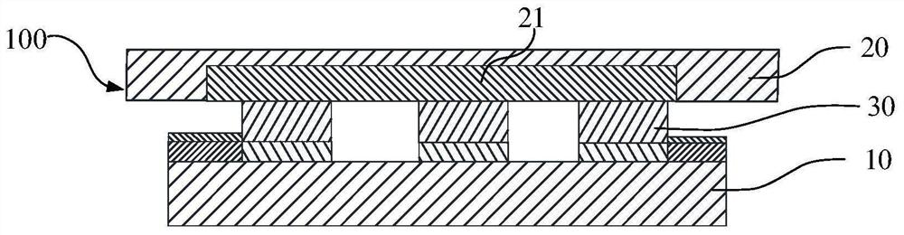
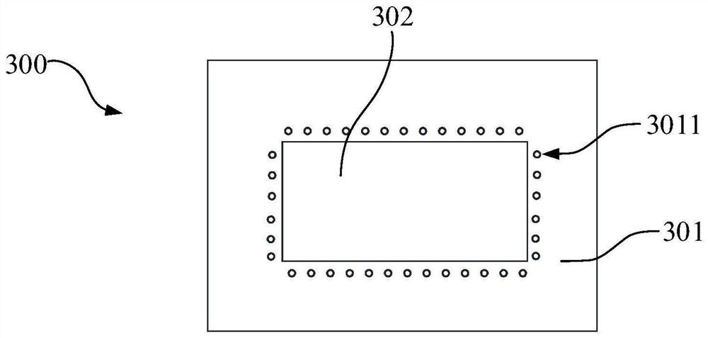
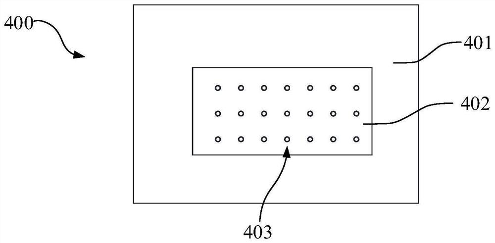
[0029] The application will be described in further detail below in conjunction with the accompanying drawings and embodiments. In particular, the following examples are only used to illustrate the present application, but not to limit the scope of the present application. Likewise, the following embodiments are only some of the embodiments of the present application but not all of them, and all other embodiments obtained by those skilled in the art without creative efforts fall within the protection scope of the present application.

[0030] Reference herein to an "embodiment" means that a particular feature, structure, or characteristic described in connection with the embodiment can be included in at least one embodiment of the present application. The occurrences of this phrase in various places in the specification are not necessarily all referring to the same embodiment, nor are separate or alternative embodiments mutually exclusive of other embodiments. It is understoo...


PUM


Abstract

The invention relates to the technical field of electronic products, and particularly relates to a PCB and a component. The PCB comprises a PCB bonding pad and a base material layer, the PCB bonding pad comprises a plurality of sub bonding pads which are arranged at intervals, and a gap channel is defined between every two adjacent sub bonding pads; the base material layer comprises a first surface and a second surface which are arranged oppositely, and the first surface is provided with a first fixing area used for fixing a plurality of sub bonding pads; and the PCB is provided with a via hole penetrating through the sub bonding pads and the base material layer, and the via hole is arranged adjacent to the gap channel and is used for conducting heat of the sub bonding pads into the second surface and the gap channel. The component comprises the PCB, a component body and a soldering tin layer, the component body comprises a component bonding pad, the soldering tin layer is located between the component bonding pad and the sub bonding pads, and then heat of the PCB bonding pad is conducted to the second surface and the gap channel through the via hole. In this way, a gas can be exhausted from the gap channel, and the welding quality is improved; and heat exchange occurs between the gap channel and the inner wall of a third via hole so that the heat conduction efficiency of the third via hole is improved.

Description

technical field [0001] This application relates to the technical field of electronic products, in particular to PCB boards and components. Background technique [0002] Components with heat dissipation pads are often used in circuit design. Such components usually have high power consumption and large heat dissipation. The printed circuit board (PCB, Printed Circuit Board) of this component needs to be designed for heat dissipation, otherwise When the temperature exceeds the tolerance range of the components, the working efficiency of the components will be reduced, or even damaged. Contents of the invention [0003] The application provides a PCB board and components. [0004] The application provides a PCB board, including: [0005] PCB pads, including a plurality of sub-pads with gaps, and gap channels are formed between adjacent sub-pads; and [0006] a substrate layer, including a first surface and a second surface disposed opposite to each other, the first surface...

Claims


Application Information

Patent Timeline
Patent Type & Authority Applications(China)
IPC IPC(8): H05K1/02H05K1/11H05K1/18
CPCH05K1/0206H05K1/111H05K1/181H05K2201/06H05K2201/0949H05K2201/094
Inventor 刘幕俊
Owner GUANGDONG OPPO MOBILE TELECOMM CORP LTD
Why Eureka
Try Eureka