Biological recognition chip surface coating treatment method

A technology of surface coating and biometric identification, which is applied in the post-processing of printing, the printing and printing of special varieties of printed matter, and can solve the problems of environmental impact of coatings, waste of raw materials, and large resource consumption.

Inactive Publication Date: 2021-07-06
苏州量子通智能科技有限公司
View PDF12 Cites 0 Cited by
  • Summary
  • Abstract
  • Description
  • Claims
  • Application Information

AI Technical Summary

Problems solved by technology

[0003] The traditional semiconductor chip adopts the method of spin coating. The advantage of the spin coating process is that it can realize automatic production, but it is mainly suitable for semiconductor biometric chips with special coating requirements, but it requires a large investment and slow cost recovery. The raw material consumption of the spin coating process is in kilograms, and the resource consumption is relatively large, resulting in waste of raw materials, and the wasted coating will also have a very large impact on the environment

Method used


Image

  • Biological recognition chip surface coating treatment method
  • Biological recognition chip surface coating treatment method
  • Biological recognition chip surface coating treatment method

Examples


example 1

[0032] Step 1: Stencil Design

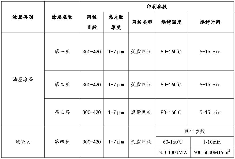
[0033] The outer diameter of the stencil is designed according to the size of the semiconductor chip. The stencil is made of a polyester stencil, and the mesh of the stencil is 300 mesh, and the thickness of the photosensitive adhesive on the stencil is designed to be 3 μm.

[0034] Step 2: Vehicle Design

[0035] Synchronously design the carrier for placing the chip into the same shape as the chip

[0036] The third step: scraper hardness setting

[0037] The scraper hardness of the silk screen is set to 75;

[0038] Step 4: Coating Printing

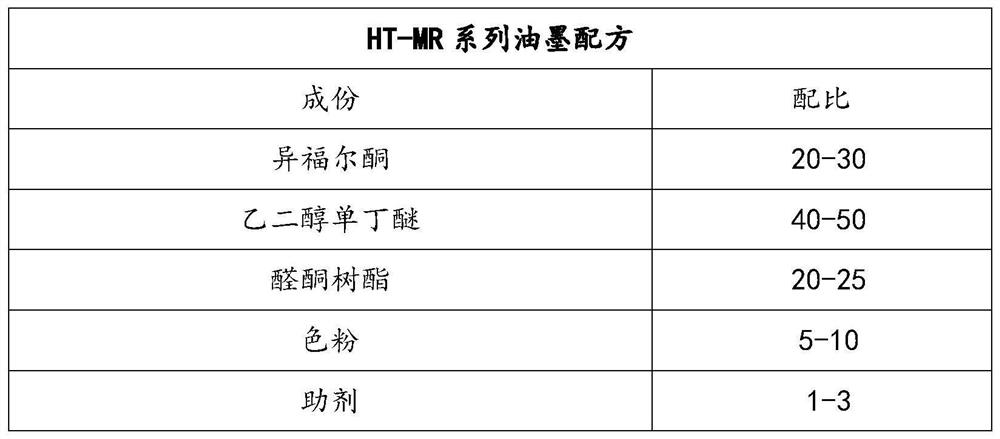
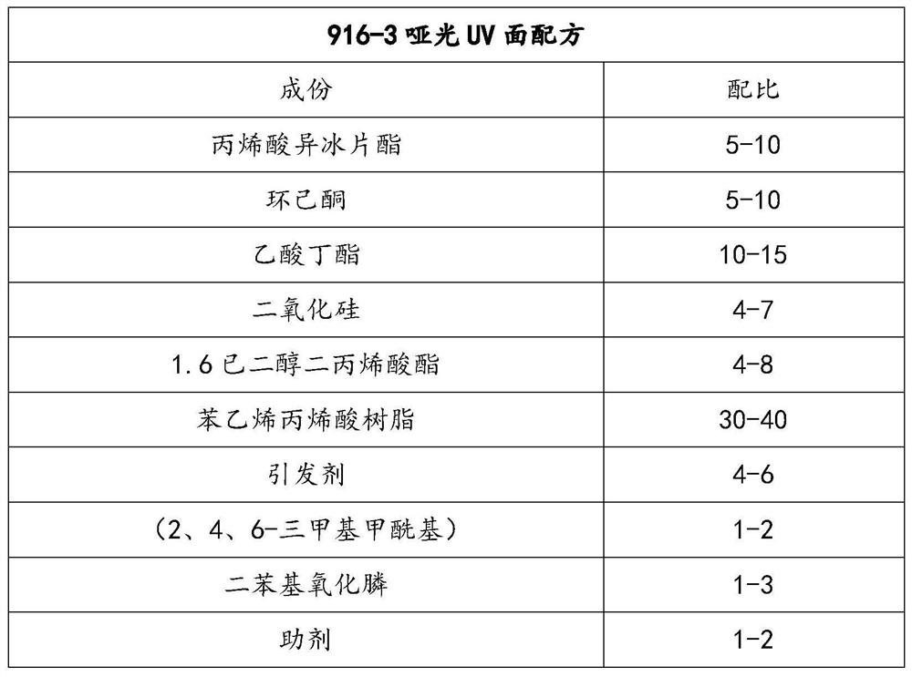
[0039] The surface of the semiconductor chip is printed with 4 layers of coating. The first layer is baked in a tunnel furnace at a temperature of 160°C for 15 minutes. The second layer is baked in a tunnel furnace at a temperature of 160°C. The baking time is 15 minutes, the third layer is baked in a tunnel oven, the baking temperature is 160°C, and the baking time is 15 minutes, the fourth layer is ...

example 2

[0041] Step 1: Stencil Design

[0042] The outer diameter of the stencil is designed according to the size of the semiconductor chip. The stencil is made of a polyester stencil, and the mesh of the stencil is 350 mesh, and the thickness of the photosensitive adhesive on the stencil is designed to be 5 μm.

[0043] Step 2: Vehicle Design

[0044] Synchronously design the carrier for placing the chip into the same shape as the chip

[0045] The third step: scraper hardness setting

[0046] The scraper hardness of the silk screen is set to 75;

[0047] Step 4: Coating Printing

[0048] The surface of the semiconductor chip is printed with 4 layers of coating. The first layer is baked in a tunnel furnace at a temperature of 160°C for 10 minutes. The second layer is baked in a tunnel furnace at a temperature of 160°C. The baking time is 10 minutes, the third layer is baked in a tunnel oven, the baking temperature is 160°C, and the baking time is 10 minutes, the fourth layer is ...

example 3

[0050] Step 1: Stencil Design

[0051] Design the outer diameter of the stencil according to the size of the semiconductor chip. The stencil is made of polyester stencil, and the mesh number of the stencil is 400 mesh, and the thickness of the photosensitive adhesive on the stencil is designed to be 6 μm.

[0052] Step 2: Vehicle Design

[0053] Synchronously design the carrier for placing the chip into the same shape as the chip

[0054] The third step: scraper hardness setting

[0055] The scraper hardness of the silk screen is set to 75;

[0056] Step 4: Coating Printing

[0057]The surface of the semiconductor chip is printed with 4 layers of coating. The first layer is baked in a tunnel furnace at a temperature of 160°C for 5 minutes. The second layer is baked in a tunnel furnace at a temperature of 160°C. The baking time is 5 minutes, the third layer is baked in a tunnel oven, the baking temperature is 160°C, and the baking time is 5 minutes, the fourth layer is bake...


PUM

PropertyMeasurementUnit
thicknessaaaaaaaaaa

Abstract

The invention discloses a biological recognition chip surface coating treatment method, and belongs to the technical field of chip printing processes. According to the biological recognition chip surface coating treatment method, through complementation of a large-area screen printing technology and a spin coating technology, chip coating with multi-color requirements can be met at the same time, the surface material of a biological recognition semiconductor chip is analyzed, the printing technology is matched with the special requirements of the surface of the semiconductor chip, self-designed raw materials are used, so that the self-design of the product is achieved, the use amount of paint in gram is achieved by deeply developing the formula of the paint, the use of the semiconductor paint is saved, the paint is more environmentally friendly in use, and the rapid production of the semiconductor biological recognition chip is successfully achieved.

Description

technical field [0001] The invention belongs to the technical field of chip printing technology, in particular to a method for treating the surface coating of a biometric recognition chip. Background technique [0002] At present, the consumer electronics industry is generally characterized by diversified product colors, diversified appearances, and short cycles; human fingerprints, facial features, palm prints, etc., have almost become biological characteristics due to their lifelong invariance, uniqueness, and convenience. A synonym for identification, human fingerprints, palm prints, etc. refer to the uneven lines on the front skin of the end of the human skin. The lines are arranged regularly to form different grain patterns. The starting point, end point, joint point and bifurcation point of the lines are called the detailed feature points of human fingerprints and palm prints. With the advent of the era of personalized appearance design of mobile devices, in order to ...

Claims


Application Information

Patent Timeline
Patent Type & Authority Applications(China)
IPC IPC(8): B41M1/12B41M3/00B41M7/00
CPCB41M1/12B41M3/00B41M7/009B41M7/0081
Inventor 王凯李基荣陈东
Owner 苏州量子通智能科技有限公司
Why Eureka
Try Eureka