semiconductor equipment

A semiconductor and equipment technology, applied in the field of semiconductor equipment, can solve the problem that the temperature measuring device cannot accurately monitor the temperature of semiconductor equipment for a long time, and achieve the effect of accurate temperature monitoring

Active Publication Date: 2022-07-22
BEIJING NAURA MICROELECTRONICS EQUIP CO LTD
View PDF5 Cites 0 Cited by
  • Summary
  • Abstract
  • Description
  • Claims
  • Application Information

AI Technical Summary

Problems solved by technology

[0006] In view of this, the present application provides a semiconductor device to solve the problem that the existing temperature measuring device cannot accurately monitor the temperature in the cavity of the semiconductor device for a long time

Method used


Image

  • semiconductor equipment
  • semiconductor equipment
  • semiconductor equipment

Examples


Embodiment Construction

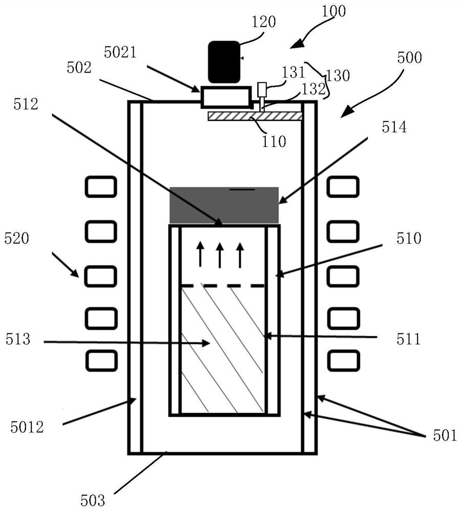
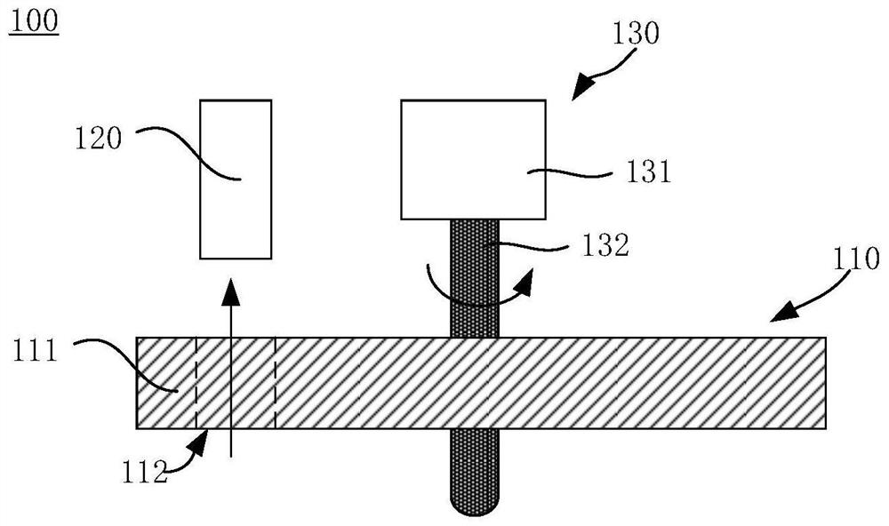
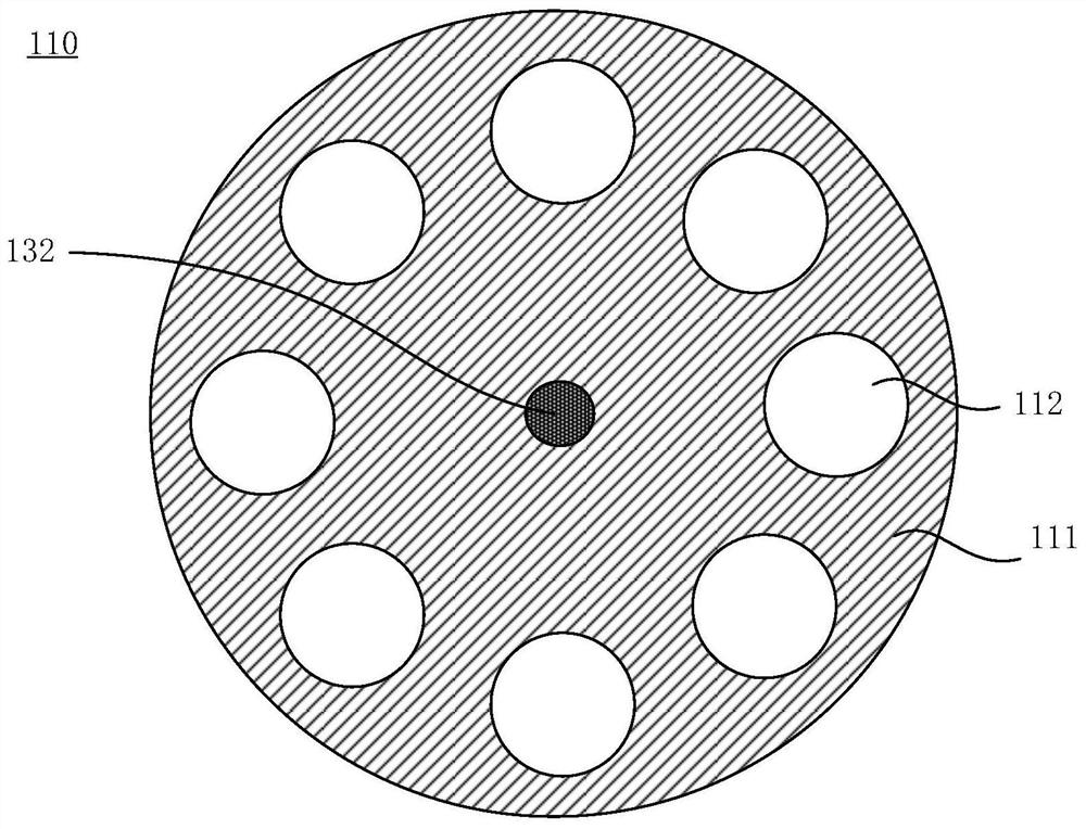
[0024] As described in the background art, in the prior art, due to the gas phase components in the physical vapor transport (PVT) growth process will be deposited on the temperature measurement window, forming a relatively dense yellow-brown volatile deposition layer, almost impermeable Light. At this time, for infrared thermometers that rely on light intensity to calculate and measure the temperature, it is no longer possible to detect the accurate temperature of the upper part of the raw material processing device, such as the crucible, through the temperature measurement window. For process monitoring, since then the temperature of the crucible has lost the ability to monitor in real time. Only electrical parameters, such as voltage, current or power, and the temperature of the cooling water, can be used as a reference, and the process experience can be used to judge whether the internal temperature of the crucible has a large temperature. Fluctuation, because the specific...


PUM

PropertyMeasurementUnit
diameteraaaaaaaaaa

Abstract

The application discloses a semiconductor device, comprising: a cavity, a first temperature measurement window is arranged on the top of the cavity; an infrared temperature measurement sensor is located outside the cavity, and the temperature measurement end of the infrared temperature measurement sensor faces the the first temperature measurement window; a temperature measurement turntable, which is located in the cavity and is fixedly arranged with the top of the cavity, and the temperature measurement turntable has at least two second temperature measurement windows; a transmission device, which is connected with the temperature measurement The turntable is connected for driving the temperature measuring turntable to rotate, rotating one of the at least two second temperature measuring windows to below the first temperature measuring window, and making the second temperature measuring window located in the on the infrared light receiving path of the infrared temperature measurement sensor, so that the infrared light radiated in the cavity passes through the second temperature measurement window and the first temperature measurement window and is received by the temperature measurement end of the infrared temperature measurement sensor . The above semiconductor device can realize long-term temperature monitoring inside the cavity.

Description

technical field [0001] The present application relates to the field of semiconductor technology, and in particular, to a semiconductor device. Background technique [0002] In recent years, with the rapid development of high-tech such as new energy vehicles and 5G technology, the demand for circuit integration density, heat dissipation performance, device breakdown resistance, and rapid switching response has become more and more intense. The performance of the next generation semiconductor - silicon (Si) has gradually been unable to meet the requirements of high performance. The third-generation semiconductors, such as gallium nitride (GaN), silicon carbide (SiC), etc., have a large band gap, high electron migration saturation rate, and excellent heat dissipation performance, breaking through the limitations of traditional silicon-based devices, making the first The third-generation semiconductors have been widely used, so the third-generation semiconductor single crystal ...

Claims


Application Information

Patent Timeline
Patent Type & Authority Patents(China)
IPC IPC(8): C30B23/00C23C14/52G01J5/02G01J5/20H01L21/67
CPCC30B23/002C23C14/52H01L21/67248G01J5/20G01J5/02
Inventor 乔建东
Owner BEIJING NAURA MICROELECTRONICS EQUIP CO LTD
Why Eureka
Try Eureka