Large-area aluminum single crystal film and preparation method and application thereof

A single-crystal thin film, large-area technology, applied in single crystal growth, single crystal growth, chemical instruments and methods, etc., can solve the problems of high dislocation density, twinning, XRD diffraction peak width, etc., and achieve a clear and sharp interface. The effect of excellent optical performance

Active Publication Date: 2021-07-13
SUZHOU INST OF NANO TECH & NANO BIONICS CHINESE ACEDEMY OF SCI
View PDF4 Cites 4 Cited by
  • Summary
  • Abstract
  • Description
  • Claims
  • Application Information

AI Technical Summary

Problems solved by technology

The results show that the growth of 100nm Al films on Si substrates has high dislocation density, resulting in broad XRD diffraction peaks or twinning

Method used


Image

  • Large-area aluminum single crystal film and preparation method and application thereof
  • Large-area aluminum single crystal film and preparation method and application thereof
  • Large-area aluminum single crystal film and preparation method and application thereof

Examples


preparation example Construction

[0030] One aspect of the embodiments of the present invention provides a method for preparing a large-area aluminum single crystal thin film, which includes:

[0031] The Si(111) substrate is sequentially subjected to organic cleaning, RCA1 cleaning, RCA2 cleaning, piranha solution cleaning and HF cleaning to obtain a pretreated Si(111) substrate;

[0032] And, under vacuum conditions, the pretreated Si(111) substrate is placed in a molecular beam epitaxy device for surface treatment at 750-800°C, and the surface of the Si(111) substrate is treated by molecular beam epitaxy technology Growing aluminum single crystal thin films to obtain large area aluminum single crystal thin films, wherein the process conditions adopted by the molecular beam epitaxy technology include: the temperature of the cold nozzle Al source is 1000-1235 °C, and the Al deposition rate is

[0033] In some more specific embodiments, the preparation method includes:

[0034]The pretreated Si(111) substra...

Embodiment 1

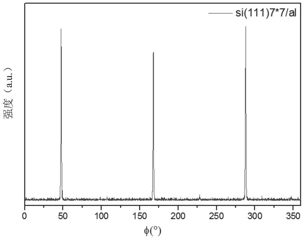
[0073] Commercial 2inch Si(111) substrates (R>10000Ω·cm) were sequentially cleaned by organic cleaning, RCA1, RCA2, piranha cleaning and HF cleaning, and then immediately put into the sample chamber of the nano-vacuum interconnection experiment station, and then introduced into the sample chamber through the ultra-high vacuum pipeline Molecular beam epitaxy (MBE), low-temperature degassing for half an hour, slowly heated to 750°C for 0.5h, clear Si(111) can be seen through high-energy electron diffraction (reflection high energy electron diffraction, RHEED) 7*7 surface, then cool down naturally, and at the same time raise the temperature of the Al source of the cold nozzle to 1000°C, at this time the Al deposition rate is about Immediately after cooling down to 100°C, an Al single crystal thin film of about 100nm is grown, which is denoted as Si(111) / Al single crystal thin film.

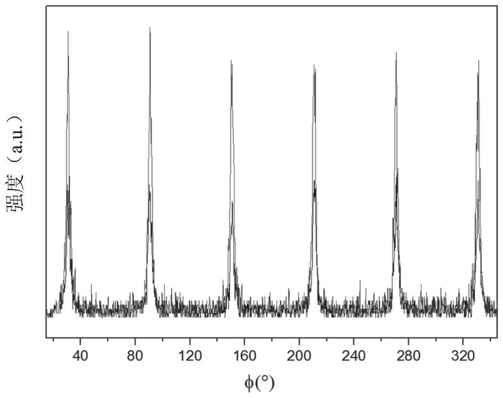
[0074] Performance characterization: The XRD spectrum of the Si(111) / Al single crystal thin film...

Embodiment 2

[0076] Commercial 2inch Si(111) substrates (R>10000Ω·cm) were sequentially cleaned by organic cleaning, RCA1, RCA2, piranha cleaning and HF cleaning, and then immediately put into the sample chamber of the nano-vacuum interconnection experiment station, and then introduced into the sample chamber through the ultra-high vacuum pipeline Molecular beam epitaxy (MBE), low-temperature degassing for half an hour, slowly heated to 770 ° C for 0.5 h, clear Si(111) can be seen through high-energy electron diffraction (reflection high energy electron diffraction, RHEED) 7*7 surface, then cool down naturally, and at the same time raise the temperature of the Al source of the cold nozzle to 1200°C, at this time the Al deposition rate is about Immediately after cooling down to 28°C, an Al single crystal thin film of about 100nm is grown, which is denoted as Si(111) / Al single crystal thin film.


PUM

PropertyMeasurementUnit
electrical resistivityaaaaaaaaaa
thicknessaaaaaaaaaa

Abstract

The invention discloses a large-area aluminum single crystal film and a preparation method and application thereof. The preparation method comprises the following steps: sequentially carrying out organic cleaning, RCA1 cleaning, RCA2 cleaning, piranha solution cleaning and HF cleaning on a Si (111) substrate to obtain a pretreated Si (111) substrate; and under a vacuum condition, placing the pretreated Si (111) substrate in a molecular beam epitaxy device for surface treatment, and growing an aluminum single crystal film on the surface of the Si (111) substrate by adopting a molecular beam epitaxy technology to obtain the large-area aluminum single crystal film. Compared with a Si substrate traditional technology, the Si (111)/Al single crystal film prepared through the method has the advantages that a large-area Al single crystal film is achieved, twin crystals do not exist, the content of C, H and O impurities on a Si/Al interface can be obviously reduced, the intrinsic quality factor of a resonator is improved to 106, and preparation of high-quality superconducting quantum bits or superconducting quantum computers is facilitated.

Description

technical field [0001] The invention belongs to the technical field of superconducting qubits, and in particular relates to a large-area aluminum single crystal thin film and its preparation method and application. Background technique [0002] The competition for quantum computer hegemony has been launched around the world, and superconducting quantum computers are taking the lead due to their compatibility with traditional micromachining technology and microwave measurement technology. The domestic 11-qubit superconducting quantum computing service was launched on the quantum computing cloud platform, and IBM realized a 50-qubit chip just last year (Arute, F., Arya, K., Babbush, R. et al. Quantum supremacy using a programmable superconducting processor.Nature574, 505-510, 2019), Google released the sensational "sycamore" chip and demonstrated "quantum supremacy", prompting us to further improve the performance of superconducting quantum chips in terms of material preparati...

Claims


Application Information

Patent Timeline
Patent Type & Authority Applications(China)
IPC IPC(8): C30B23/02C30B29/02G06N10/00
CPCC30B29/02C30B23/025G06N10/00
Inventor 武彪冯加贵熊康林陈建孙骏逸黄永丹朱博杰丁孙安陆晓鸣
Owner SUZHOU INST OF NANO TECH & NANO BIONICS CHINESE ACEDEMY OF SCI
Why Eureka
Try Eureka