A drive power circuit and its drive method
A technology for driving power supply and charging circuit, which is applied in the direction of program control, instrument, computer control, etc. It can solve the problems of large influence of temperature change and load change, temperature rise of related charging and discharging devices, complex calculation and control, etc., to improve the system Reliability, lower device temperature rise, simple driving effect
- Summary
- Abstract
- Description
- Claims
- Application Information
AI Technical Summary
Problems solved by technology
Method used
Image
Examples
no. 1 example
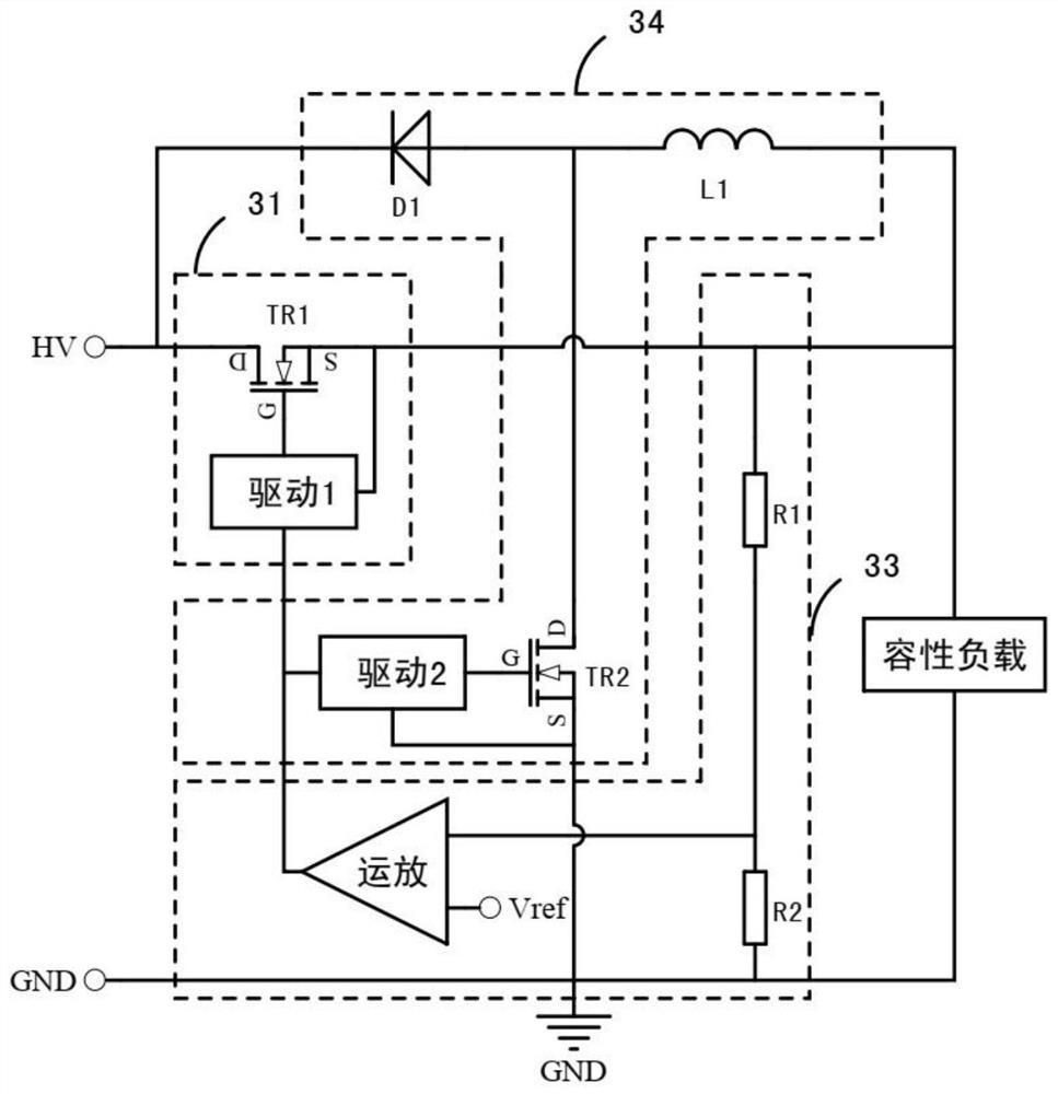
[0038] The output voltage generating module circuit of the first embodiment of the present invention is as follows Figure 4 As shown, the charging circuit 31 includes a MOS transistor TR1, a resistor R3, an optocoupler OC1 and a diode D2, the comparison circuit 33 includes an operational amplifier, a capacitor C1, a sampling resistor R1 and a sampling resistor R2, and the discharge circuit 34 includes an inductor L1, a diode D1, a MOS Tube TR2, resistor R4, transistor Q1 and resistor R5.
[0039] The drain of the MOS transistor TR1 is used to connect the output terminal of the main power supply module of the power supply module 1, the source of the MOS transistor TR1 is used to connect the comparison circuit and the capacitive load, the resistor R3 is connected between the gate and the source of the MOS transistor TR1, and the MOS transistor The gate of TR1 is connected to the negative output terminal of the optocoupler OC1. The positive output terminal of the optocoupler OC1...
no. 2 example
[0049] The output voltage generating module circuit of the second embodiment of the present invention is as follows: Figure 4 As shown, compared with the first embodiment, the difference is that the discharge circuit 35 (34) adopts a flyback structure, including a transformer T1, a diode D1, a MOS transistor TR2, a resistor R4, a resistor R5 and a transistor Q1, and the transformer T1 is a primary synonym The terminal is connected to one terminal of the capacitive load and the connection point of the comparison circuit 33, the primary terminal of the transformer T1 is connected to the drain of the MOS transistor TR2, the source terminal of the MOS transistor TR2 is connected to the ground, the secondary terminal of the transformer T1 is connected to the anode of the diode D1, and the secondary terminal of the transformer T1 is different. The name terminal is connected to the ground, the cathode of the diode D1 is used to connect the output terminal of the main power supply mod...
PUM
 Abstract
Description
Claims
Application Information


