Check patentability & draft patents in minutes with Patsnap Eureka AI!

Static random access memory cell

A static random access and memory unit technology, applied in static memory, digital memory information, information storage, etc., can solve problems such as complex metal routing of double-ended SRAM units

Pending Publication Date: 2021-07-13
TAIWAN SEMICON MFG CO LTD
View PDF0 Cites 0 Cited by
  • Summary
  • Abstract
  • Description
  • Claims
  • Application Information

AI Technical Summary

Problems solved by technology

Dual-terminal SRAM cells may have complex metal routing, which may pose challenges for routing setup and lithography process window

Method used


Image

  • Static random access memory cell
  • Static random access memory cell
  • Static random access memory cell

Examples


Embodiment Construction

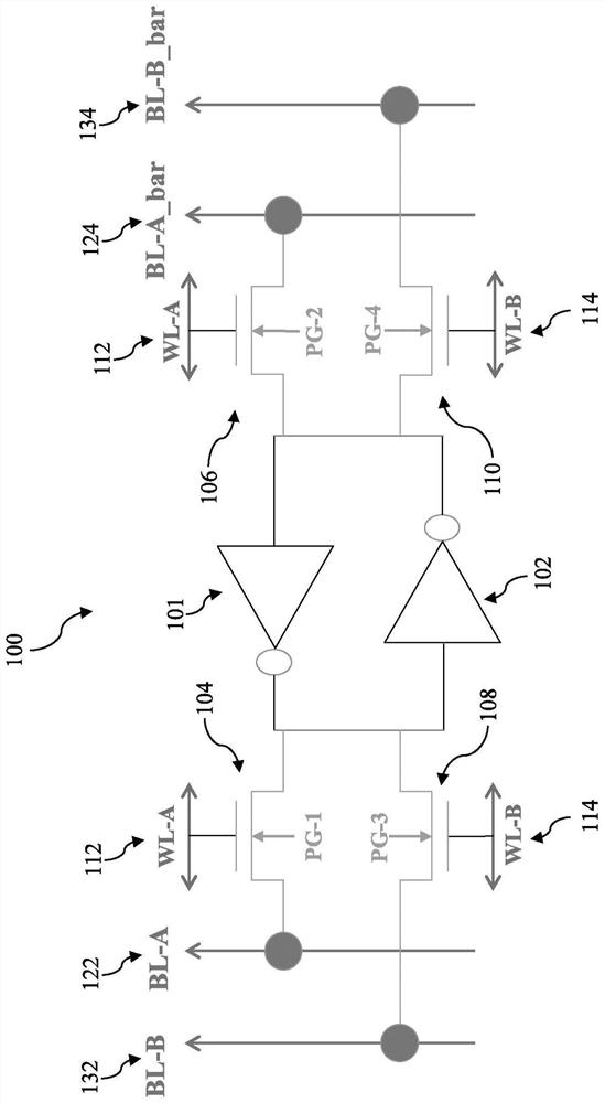
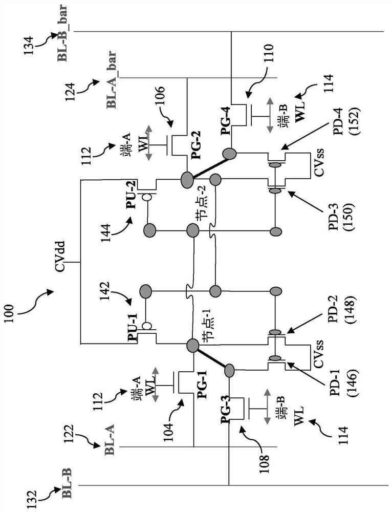
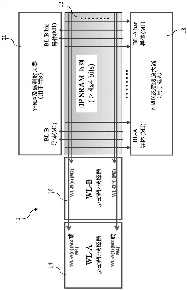
[0123] The following disclosure provides many different embodiments, or examples, for implementing different features of the disclosure. Specific examples of the various components and arrangements of the present disclosure are described below to simplify the description. Of course, these examples are not intended to limit the present disclosure. For example, if a first feature is described as being formed on or over a second feature, it may include embodiments where the first and second features are formed in direct contact, or may include additional features formed on the first feature An embodiment in which the first feature and the second feature are not in direct contact with the second feature. Additionally, the present disclosure may repeat reference numbers and / or letters in various instances. This repetition is for simplicity and clarity and does not in itself dictate the relationship between the various embodiments and / or configurations discussed.

[0124] Additio...


PUM


Abstract

A static random access memory (SRAM) cell of the present disclosure includes a first pull-down device, a second pull-down device, a first transfer gate device, and a second transfer gate device disposed in a first p-well on a substrate; a third pull-down device, a fourth pull-down device, a third transmission gate device and a fourth transmission gate device which are arranged in a second p well on the substrate; a first pull-up device and a second pull-up device which are disposed in an n-well disposed between the first p-well and the second p-well; and a first landing pad between the second pull-down device and the first pull-up device. The first landing pad is electrically coupled to the gate structure of the second transfer gate device via a path of the first gate via.

Description

technical field [0001] The present disclosure relates to a static random access memory (SRAM) cell, and more particularly to a SRAM cell having orthogonal metal lines. Background technique [0002] The semiconductor industry has experienced rapid growth. Advances in technology in semiconductor materials and design have produced several generations of semiconductor devices, each generation having smaller and more complex circuits than the previous generation. During the development of integrated circuits (ICs), functional density (eg, the number of interconnected devices per unit chip area) typically increases, while geometric dimensions (eg, the The smallest component (or line) will shrink. This scaling process typically provides benefits by increasing production efficiency and reducing associated costs. However, these advances do increase the complexity of the process and manufacture of semiconductor devices. [0003] In deep sub-micron integrated circuit technology, em...

Claims


Application Information

Patent Timeline
IPC IPC(8): G11C5/06G11C11/41G11C11/413
CPCG11C5/06G11C11/41G11C11/413H01L27/0207H01L27/0924H10B10/12
Inventor 廖忠志
Owner TAIWAN SEMICON MFG CO LTD
Features
  • R&D
  • Intellectual Property
  • Life Sciences
  • Materials
  • Tech Scout
  • Unparalleled Data Quality
  • Higher Quality Content
  • 60% Fewer Hallucinations
Learn More