System and method for establishing simulation model of field effect transistor

A field effect transistor and simulation model technology, applied in special data processing applications, instruments, calculations, etc., can solve problems such as excessive gate current, SPICE simulation convergence problems, affecting the accuracy of JFET models, and ensure accurate simulation. effect of good model properties

Active Publication Date: 2022-05-17
上海华大九天信息科技有限公司
View PDF0 Cites 0 Cited by
  • Summary
  • Abstract
  • Description
  • Claims
  • Application Information

AI Technical Summary

Problems solved by technology

[0003] In the SPICE model of a conventional JFET, a parasitic diode is built between the gate and the source. When the voltage between the gate and the source is large, the gate current will be too large, which will cause convergence problems in SPICE simulation. Unable to accurately analyze the parameter characteristics of the model
Although the series resistance of the gate can alleviate the convergence problem, it will affect the characteristics of the model's current / capacitance variation with voltage, which will seriously affect the accuracy of the JFET model.
Therefore, the simulation accuracy of the current JFET model is not high

Method used


Image

  • System and method for establishing simulation model of field effect transistor
  • System and method for establishing simulation model of field effect transistor
  • System and method for establishing simulation model of field effect transistor

Examples


Embodiment Construction

[0035] Various embodiments of the invention will be described in more detail below with reference to the accompanying drawings. In the various drawings, the same elements are denoted by the same or similar reference numerals. For the sake of clarity, various parts in the drawings have not been drawn to scale. Also, some well-known parts may not be shown.

[0036] In the present application, the term "semiconductor structure" refers to a general designation of the entire semiconductor structure formed in various steps of manufacturing a semiconductor device, including all layers or regions that have been formed.

[0037] The specific implementation manners of the present invention will be further described in detail below in conjunction with the accompanying drawings and embodiments.

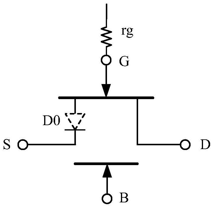
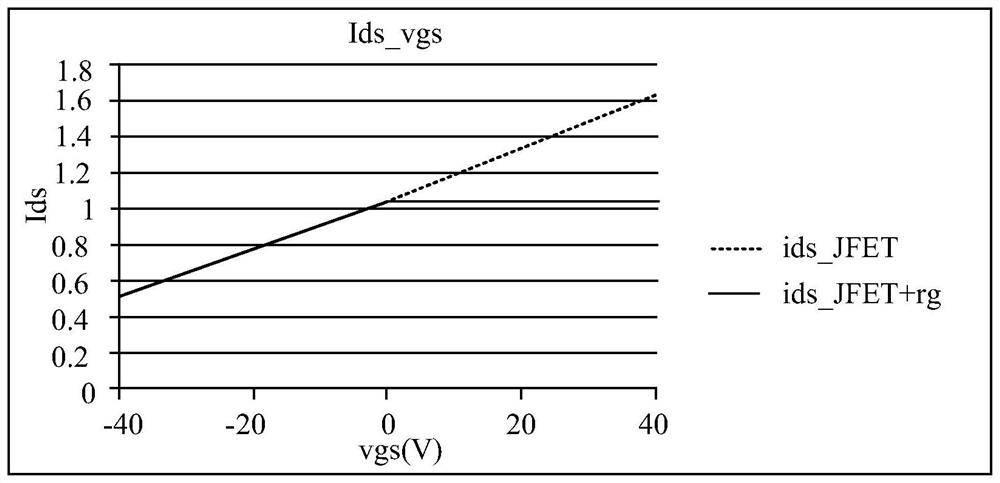
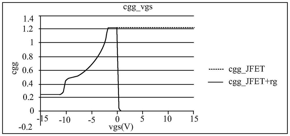
[0038] figure 1 Schematic diagram of the simplified structure of the JFET model showing the gate series resistance; Figure 2a and Figure 2b respectively show the basis of figure 1 The cur...


PUM


Abstract

A system and method for establishing a simulation model of a field effect transistor are disclosed. The simulation model of the field effect transistor includes: a field effect transistor model, including four gate electrodes, source electrodes, drain electrodes, and body electrodes of the field effect transistor. Connection terminal; the first diode model, including the first diode, connected between the body electrode and the drain of the field effect transistor model; the second diode model, including the second diode, connected between the field effect transistor model Between the body electrode and the source, the first diode model and the second diode model characterize the leakage characteristics and capacitance voltage characteristics of the field effect transistor through breakdown voltage parameters and temperature parameters. The simulation model of the field effect transistor characterizes the leakage characteristics and capacitance voltage characteristics of the field effect transistor through the breakdown voltage parameters and temperature parameters, so that the model can better reflect the device characteristics, solve the convergence problem and ensure the accuracy of the simulation.

Description

technical field [0001] The invention relates to the technical field of device simulation, in particular to a system for establishing a simulation model of a field effect transistor and a method for establishing the same. Background technique [0002] Junction Field-Effect Transistor (JFET) is an active device with amplification function, which is widely used in circuit design and is also used to manufacture various semiconductor devices. In order to speed up the manufacturing cycle and avoid waste of resources, the circuit or semiconductor device is usually modeled and simulated before it is put into production, and the established device model is simulated by using SPICE simulation tools to obtain different fitting curves, so that it can be quickly Analyze whether the device can work normally, and whether the parameters are good. [0003] In the SPICE model of a conventional JFET, a parasitic diode is built between the gate and the source. When the voltage between the gate...

Claims


Application Information

Patent Timeline
Patent Type & Authority Patents(China)
IPC IPC(8): G06F30/367
CPCG06F30/367Y02E60/00
Inventor 傅飞朱能勇
Owner 上海华大九天信息科技有限公司
Why Eureka
Try Eureka