Optimized digital wireless communication chip system

A communication chip and digital wireless technology, applied in the direction of electrical digital data processing, special data processing applications, instruments, etc., can solve problems affecting the performance of digital wireless communication chips, complex algorithms of wireless communication systems, and elegant layout and wiring, etc., to achieve Provides radio frequency performance, simplifies board layout rules, and low cost

Pending Publication Date: 2021-07-20
武汉工控仪器仪表有限公司
View PDF0 Cites 0 Cited by
  • Summary
  • Abstract
  • Description
  • Claims
  • Application Information

AI Technical Summary

Problems solved by technology

[0005] In order to overcome the defects of existing digital wireless communication chips such as high application threshold, sophisticated layout and routing, complex algorithms and great difficulty in building a stable wireless communication system, which greatly affect the performance of digital wireless communication chips, the purpose of the present invention is to provide An improved digital wireless communication chip system that can overcome the defects of the prior art

Method used


Image

  • Optimized digital wireless communication chip system
  • Optimized digital wireless communication chip system
  • Optimized digital wireless communication chip system

Examples


Embodiment Construction

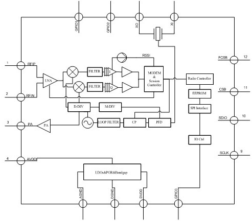
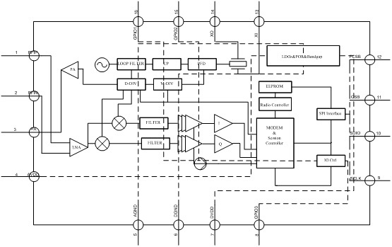
[0025] refer to figure 1 , The digital wireless communication chip system includes a radio frequency controller and EEPROM connected to it, data buffer FIFO, SPI interface, IO controller, RSSI detector, IQ demodulator, LNA, mixer, PA, PLL, VCO, QFN16 package.

[0026] The radio frequency controller adopts an FPGA, the EEPROM is an 8*128bit power-down storage and electric erasable memory array, the data buffer FIFO is a 8*64bits RAM, and the SPI interface is a logical main SPI interface , through CSB, FCSB, SCLK, SDIO four-wire connection to the RF controller, CSB, FCSB, SCLK, SDIO four-wire routing without special process, the connection is only for connection; the IO controller includes logic input and The output circuit is connected to the chip package pins GPIO1, GPIO2, and GPIO3; the RSSI detector is connected to the radio frequency controller, the IQ demodulator is connected to the radio frequency controller through an IPC channel, and the LNA is directly connected to T...


PUM


Abstract

The invention relates to the field of digital wireless communication chips, in particular to an optimized digital wireless communication chip system, which comprises a radio frequency controller, and an EEPROM, a data cache FIFO, an SPI interface, an IO controller, an RSSI detector, an IQ demodulator, an LNA, a mixer, a PA, a PLL, a VCO and a QFN16 package connected with the radio frequency controller. The SPI interface is a logic main SPI interface, and is connected to the radio frequency controller through four lines, namely a CSB, an FCSB, an SCLK and an SDIO; the IO controller comprises a logic input circuit and a logic output circuit which are connected with chip packaging pins GPIO1, GPIO2 and GPIO3; the RSSI detector is connected with the radio frequency controller, the IQ demodulator is connected with the radio frequency controller through an IPC channel, the LNA is directly connected to an antenna input end, the mixer is connected with the LNA and the VCO through a chip internal shielding circuit, and the PA is connected with an antenna output end and the VCO. The board arrangement and wiring rule of chip application is greatly simplified.

Description

technical field [0001] The invention relates to the field of digital wireless communication chips, in particular to an optimized digital wireless communication chip system. Background technique [0002] The existing digital communication chip is a highly integrated and intelligent integrated circuit. Digital communication chips are widely used in various smart home products, industrial security products, aerospace, military facilities, and police equipment in modern society. Key devices are the premise and foundation of social modernization. [0003] There are many digital wireless communication chip products on the market, with different manufacturers and great product differences, but there is generally a problem of application threshold. Regardless of whether it is a large foreign manufacturer or a domestic chip, it is necessary to consider the layout and routing during design to avoid crosstalk and unnecessary electromagnetic radiation as much as possible. [0004] Mos...

Claims


Application Information

Patent Timeline
Patent Type & Authority Applications(China)
IPC IPC(8): G06F30/3308
CPCG06F30/3308
Inventor 汪银心王鹏
Owner 武汉工控仪器仪表有限公司
Why Eureka
Try Eureka