
A Large Size Ceramic Package Interface Structure

A technology of ceramic encapsulation and interface structure, applied in the direction of insulators, etc., can solve the problems such as the inability to effectively ensure the air-tightness of the large-sized vacuum insulation interface, the reduction of the vacuum performance of the vacuum insulation interface, and the large thermal expansion difference between the metal and the ceramic, etc. The effect of reducing the risk of explosion and improving reliability

Active Publication Date: 2022-05-31
SOUTHWEST CHINA RES INST OF ELECTRONICS EQUIP
View PDF0 Cites 0 Cited by
  • Summary
  • Abstract
  • Description
  • Claims
  • Application Information

AI Technical Summary

Problems solved by technology

[0004] 1. Due to the large diameter of the ceramic, the unreasonable ceramic and metal sealing structure will directly cause the ceramic to burst during the sealing process;
[0005] 2. The existing technology cannot effectively guarantee that the large-size vacuum insulation interface does not leak air under the baking condition of the maximum temperature of 200 ° C for 5 hours;
[0006] 3. In the process of ceramic sealing, the amount of brazing material is too large, and the positioning is difficult;
[0007] 4. When brazing and sealing, the thermal expansion difference between metal and ceramics is large, and the solder is easy to lose after melting, resulting in insufficient filling in some areas, and eventually resulting in excessive leakage rate in the sealing area;
[0008] 5. In the existing large-size ceramic packaging structure, the brazed sealing surface and the welded joint generally appear at the same time. If the design of the welded joint is unreasonable, it will cause new leaks on the brazed surface and reduce the vacuum of the vacuum insulation interface. performance

Method used


Image

  • A Large Size Ceramic Package Interface Structure
  • A Large Size Ceramic Package Interface Structure
  • A Large Size Ceramic Package Interface Structure

Examples


Embodiment Construction

[0039] In the present invention, unless otherwise expressly specified and limited, the terms "installed", "connected", "connected", "fixed", etc.

[0040] The present invention will be described in detail below.

[0049] In some possible embodiments, the side of the cylinder one 401 away from the support ring is provided with an annular protrusion,

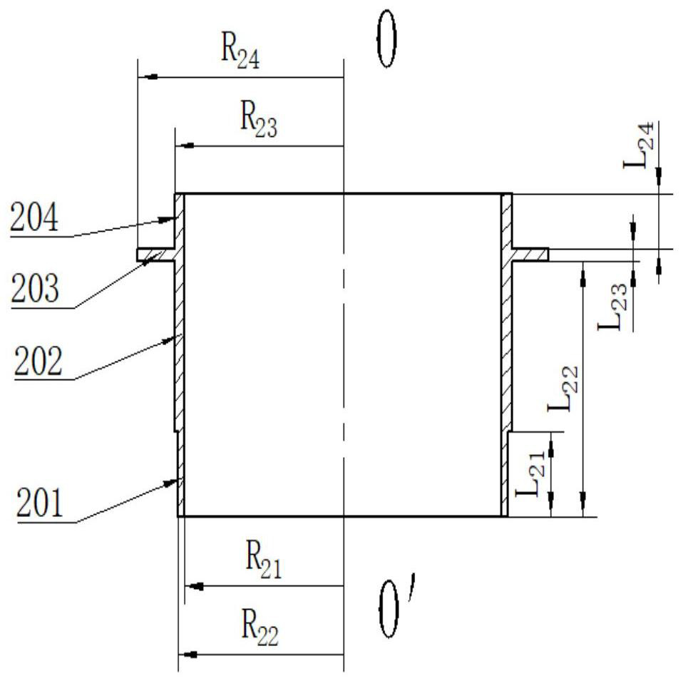
[0050] FIG. 4 is a schematic cross-sectional view of the inner conductor support base 4 of the present invention along the front direction of OO'. The inner conductor support seat 4 consists of a cylinder 401,

[0067] In some possible embodiments, in order to facilitate the installation and positioning of the ceramic during the brazing seal, and to facilitate

[0078] The present invention is not limited to the foregoing specific embodiments. The present invention extends to any of the


PUM


Abstract

The invention belongs to the technical field of pulse power, and specifically discloses a large-size ceramic packaging interface structure, including an insulator provided with a round hole, an inner kovar ring set in the round hole, a stress-relieving ceramic ring, and an inner kervar ring set in the round hole. The inner inner conductor support seat, the outer kovar ring set on the outside of the insulator; a ring-shaped installation cavity is formed between the inner kovar ring and the inner conductor support seat, and the stress-relieving ceramic ring is installed in the ring-shaped installation cavity . The invention can effectively reduce the possibility of air leakage at the interface of the ceramic packaging under the long-time baking condition at 200°C, improve the vacuum degree and vacuum maintenance ability of the system, and has a compact structure and is easy to manufacture.

Description

A large-scale ceramic package interface structure technical field The invention belongs to the technical field of pulse power, be specifically related to a kind of large-size ceramic seal for high-voltage coaxial transmission Install interface structure. Background technique Between the output end of the pulsed power source and the high-power microwave electric vacuum device, an achievable coaxial The insulating interface of transmission to isolate the pulse transmission line and the electric vacuum device, this interface should not only withstand the working medium in the pulse power source The generated static pressure greater than 0.5MPa is also used as the vacuum interface of the microwave electric vacuum device. Ceramic metal seal The way of connecting the structure is an ideal solution to ensure the structural strength of the insulating interface and improve the vacuum performance of the microwave vacuum device. Law. [0003] With the improvement of the desi...

Claims


Application Information

Patent Timeline
Patent Type & Authority Patents(China)
IPC IPC(8): H01B17/60
CPCH01B17/60
Inventor 漆中华陈宏刘正勇张永红侯吉来肖开奇王亮王伟年侯朝睿陶莲娟贺江华袁泽龙
Owner SOUTHWEST CHINA RES INST OF ELECTRONICS EQUIP
Learn More