
Novel GaN-based ESD protection circuit

A protection circuit, a new type of technology, applied in circuits, electrical components, electric solid devices, etc., can solve the problems of inability to provide bidirectional protection, unidirectional protection, etc., and achieve the effect of reducing leakage current, reducing power consumption, and reducing the difficulty of manufacturing process

Inactive Publication Date: 2021-07-23
UNIV OF ELECTRONICS SCI & TECH OF CHINA
View PDF5 Cites 6 Cited by
  • Summary
  • Abstract
  • Description
  • Claims
  • Application Information

AI Technical Summary

Problems solved by technology

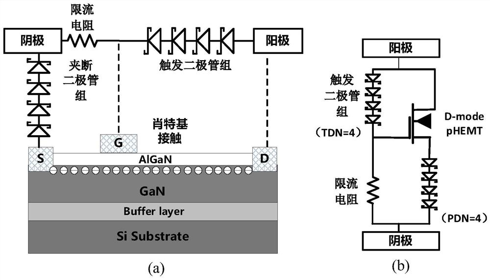
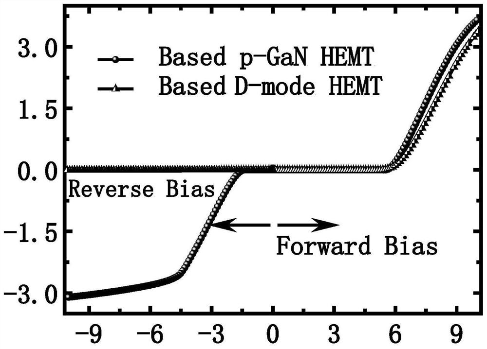
However, due to the existence of the pinch-off diode group, this type of protection scheme can only provide one-way protection, and cannot provide two-way protection

Method used


Image

  • Novel GaN-based ESD protection circuit
  • Novel GaN-based ESD protection circuit
  • Novel GaN-based ESD protection circuit

Examples


Embodiment Construction

[0018] The present invention will be described in detail below in conjunction with the accompanying drawings.

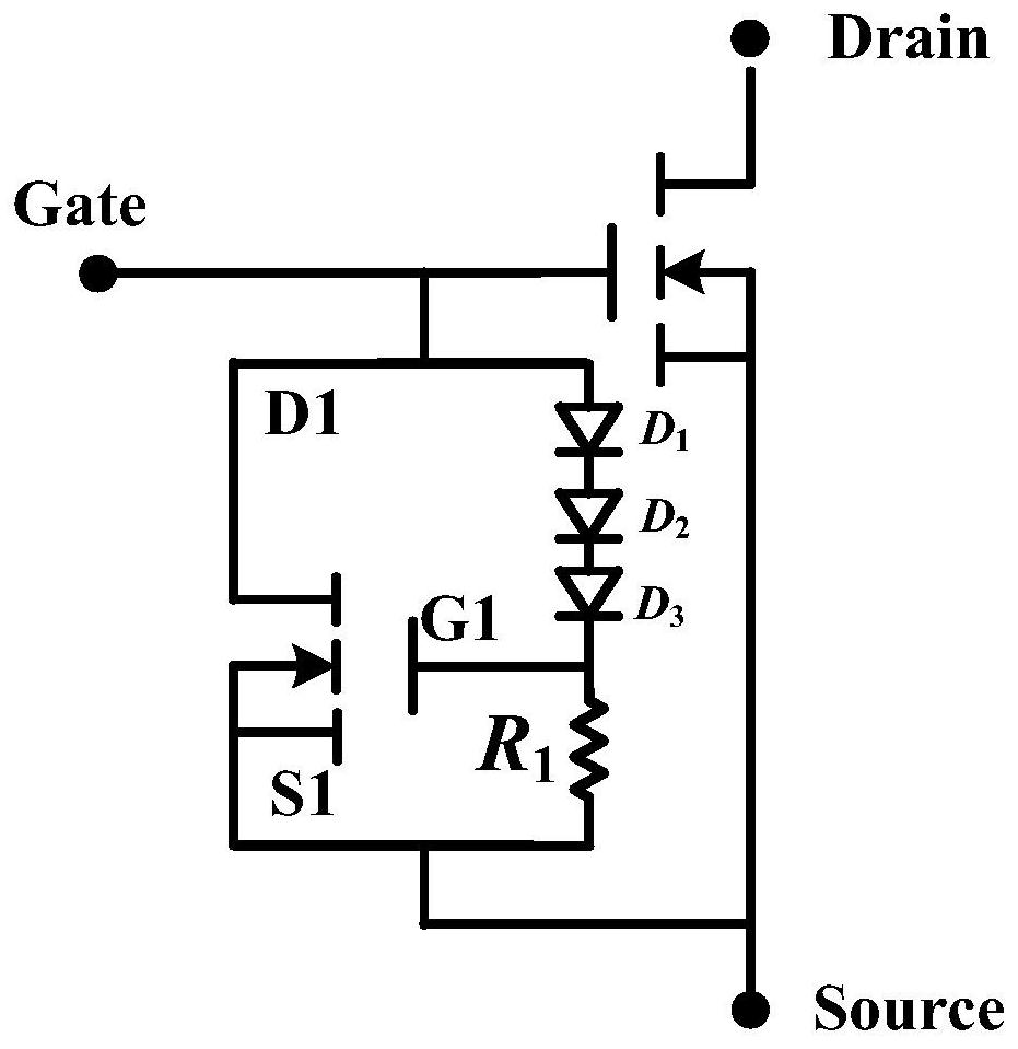
[0019] Such as figure 2 As shown, the present invention is composed of an enhanced p-GaN HEMT device, a current limiting resistor and a trigger diode group. Among them, the gate of the p-GaN enhanced device is an ohmic contact type, and the trigger diode group is four normally-off field-controlled power diodes. The field control diode can be regarded as a p-GaN HEMT gate and drain shorted together, and then a voltage is applied to the drain, when the voltage applied to the drain exceeds the threshold voltage V TH Finally, the channel under the gate is turned on, and then the drain current increases with the increase of the applied drain current. In this working mode, it is consistent with the working characteristics of the diode, so it is also called normally-off field-controlled power diode. When the protection circuit composed of the above components is connect...


PUM


Abstract

The invention belongs to the technical field of semiconductor devices and integrated circuits, and particularly relates to a GaN-based ESD protection circuit. Different from a conventional ESD protection circuit composed of a diode group, the ESD protection circuit is composed of an enhanced p-GaN HEMT device, a GaN-based trigger diode group and a current-limiting resistor. Reverse conduction can be achieved when the gate and the source of the enhanced p-GaN HEMT device have the same potential, so that the bidirectional protection function which a diode group protection circuit does not have is realized. Meanwhile, under the same protection level, compared with a diode group protection circuit, the leakage current can be reduced, and the power consumption caused by the leakage current can be reduced. In addition, the preparation process is compatible with the enhanced p-GaN HEMTs process, so that the preparation process difficulty when the ESD protection circuit is integrated with a protected device can be greatly reduced. The ESD protection circuit is suitable for circuits of enhanced p-GaN HEMTs gate protection, input and output ports of GaN radio frequency power amplifiers and the like.

Description

technical field [0001] The invention belongs to the technical field of semiconductor devices and integrated circuits, and in particular relates to a novel GaN-based ESD protection circuit. Background technique [0002] Gallium Nitride (GaN) is a representative of the third-generation wide-bandgap semiconductor material, and has attracted extensive attention from researchers from various countries. GaN materials have the characteristics of large forbidden band width, high saturated electron drift velocity, small dielectric constant and good chemical stability. Therefore, compared with Si-based devices, GaN-based HEMT devices have lower on-resistance, smaller Excellent properties such as parasitic capacitance and high breakdown voltage can meet the application requirements of the next generation system for semiconductor devices with higher power, smaller volume and higher frequency. [0003] However, the traditional AlGaN / GaN heterojunction-based devices are depletion-mode de...

Claims


Application Information

Patent Timeline
Patent Type & Authority Applications(China)
IPC IPC(8): H01L27/02
CPCH01L27/0266H01L27/0255H01L27/0288
Inventor 陈万军王园段力冬信亚杰张波
Owner UNIV OF ELECTRONICS SCI & TECH OF CHINA
Learn More