Unlock instant, AI-driven research and patent intelligence for your innovation.

Analog-to-digital converter device and clock pulse skew correction method

An analog-to-digital conversion and analog-to-digital technology, which is applied in the field of time-interleaved analog-to-digital converters and clock skew correction, can solve problems affecting resolution or linearity, gain error, and high cycle required for ADC power consumption correction. Achieve the effect of reducing power consumption and calibration cycle

Active Publication Date: 2021-07-23
GLOBAL UNICHIP CORPORATION +1
View PDF5 Cites 0 Cited by
  • Summary
  • Abstract
  • Description
  • Claims
  • Application Information

AI Technical Summary

Problems solved by technology

In practical applications, ADC will affect its own resolution or linearity due to gain error, voltage error or timing error
Among them, for the timing error, the existing technology needs to set up complex circuits (such as additional reference ADC circuit, auxiliary ADC circuit) or use off-chip correction to correct, so that the power consumption of the ADC or is the correction period required for higher and higher

Method used


Image

  • Analog-to-digital converter device and clock pulse skew correction method
  • Analog-to-digital converter device and clock pulse skew correction method
  • Analog-to-digital converter device and clock pulse skew correction method

Examples


Embodiment Construction

[0067] Embodiments of the present invention will be described below in conjunction with related drawings. In the drawings, the same reference numerals represent the same or similar elements or method flows.

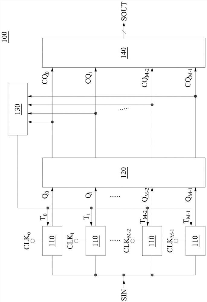
[0068] see Figure 1A and Figure 1B , Figure 1A It is a schematic diagram of an analog-to-digital converter (analog-to-digital converter, ADC) device 100 according to some embodiments of the present application. Figure 1B according to some embodiments of this case Figure 1A Multiple clock signals CLK in 0 ~CLK M-1 The schematic diagram of the waveform. In some embodiments, the ADC device 100 operates as a time-interleaved ADC with multiple channels.

[0069] In some embodiments, the ADC device 100 includes a plurality of analog-to-digital conversion circuits 110 , a correction circuit 120 , a skew adjustment circuit 130 and an output circuit 140 . It should be noted that each ADC circuit 110 operates as a single channel. In other words, in this example, the ADC ...


PUM


Abstract

The invention discloses an analog-to-digital converter device and a clock pulse skew correction method. The analog-to-digital converter device includes a plurality of analog-to-digital conversion circuits, a correction circuit, and a skew adjustment circuit. The plurality of analog-to-digital conversion circuits are configured to convert an input signal according to a plurality of interleaved clock pulse signals to generate a plurality of first quantified outputs. The correction circuit is configured to perform at least one correction operation according to the first quantified outputs to generate a plurality of second quantified outputs. The skew adjustment circuit is configured to determine a plurality of calculation signals corresponding to the respective second quantified outputs in a predetermined period, average the calculation signals to generate a reference signal, compare the reference signal with the calculation signals separately to generate a plurality of detection signals, and determine whether to adjust the detection signals according to the signal frequency to generate a plurality of adjustment signals, wherein the adjustment signals are used for reducing clock pulse skew of the analog-to-digital conversion circuits. Therefore, the effects of reducing the overall power consumption and correcting the period are achieved.

Description

technical field [0001] This case relates to an analog-to-digital converter device, and in particular to a time-interleaved analog-to-digital converter and its clock skew correction method. Background technique [0002] Analog-to-digital converters (analog-to-digital converters, ADCs) are commonly used in various electronic devices for converting analog signals to digital signals for signal processing. In practical applications, the resolution or linearity of the ADC will be affected by gain errors, voltage errors or timing errors. Among them, for the timing error, the existing technology needs to set up complex circuits (such as additional reference ADC circuit, auxiliary ADC circuit) or use off-chip correction to correct, so that the power consumption of the ADC or It is that the period required for correction is getting higher and higher. Contents of the invention [0003] The first implementation aspect of the present case is to provide an analog-to-digital converter ...

Claims


Application Information

Patent Timeline
Patent Type & Authority Applications(China)
IPC IPC(8): H03M1/10
CPCH03M1/1028
Inventor 康文柱陈昱竹汪鼎豪
Owner GLOBAL UNICHIP CORPORATION