Display panel and packaging structure preparation method for display panel

A display panel and packaging structure technology, which is applied in semiconductor/solid-state device manufacturing, semiconductor devices, electrical components, etc., can solve the problems of gas barrier layer microcracks, stress concentration, bubble generation, etc., to improve easy failure and service life , Enhance the effect of encapsulation effect

Active Publication Date: 2022-05-31
SHENZHEN CHINA STAR OPTOELECTRONICS SEMICON DISPLAY TECH CO LTD
View PDF13 Cites 0 Cited by
  • Summary
  • Abstract
  • Description
  • Claims
  • Application Information

AI Technical Summary

Problems solved by technology

[0005] The invention provides a display panel and a method for preparing a packaging structure of the display panel, which can solve the problem of using an adhesive to isolate a light-emitting device and a glass substrate from the atmosphere in the prior art, or to use vapor deposition on the substrate after covering the light-emitting device. Form a gas barrier layer. In order to prevent water vapor intrusion, use a material with low moisture permeability to form a gas barrier layer. Use a sealed UV resin to form a sealed space around the substrate to block water and oxygen intrusion. When using an adhesive layer, bubbles will be generated, increasing After the resin filling layer, because the curing of the resin material will cause bending deformation of the substrate, or form a thicker gas barrier layer, after the step difference is generated, stress concentration will be caused, and microcracks will easily occur in the gas barrier layer

Method used


Image

  • Display panel and packaging structure preparation method for display panel
  • Display panel and packaging structure preparation method for display panel
  • Display panel and packaging structure preparation method for display panel

Examples


Embodiment Construction

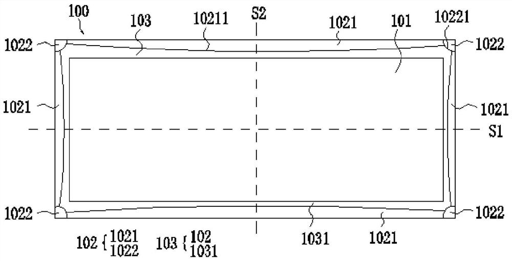
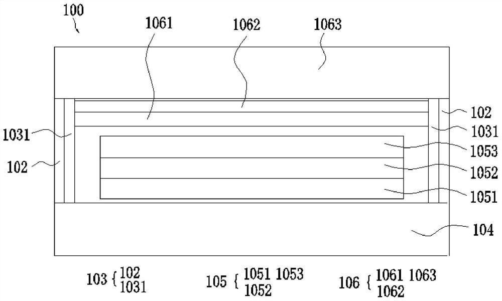
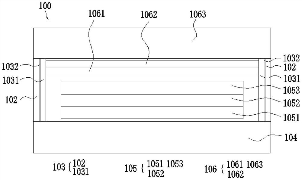
[0029] The following descriptions of the various embodiments refer to the accompanying drawings to illustrate specific embodiments in which the invention may be practiced. The directional terms mentioned in the present invention, such as [up], [down], [front], [rear], [left], [right], [inner], [outer], [side], etc., are only for reference Additional schema orientation. Therefore, the directional terms used are for describing and understanding the present invention, not for limiting the present invention. In the figures, units with similar structures are denoted by the same reference numerals, and the dotted lines in the figures indicate that they do not exist in the structures, and only illustrate the shapes and positions of the structures.

[0030] The present invention aims at using an adhesive to isolate the light-emitting device and the glass substrate from the atmosphere in the prior art, or after covering the light-emitting device, a gas barrier layer is formed on the s...


PUM

PropertyMeasurementUnit
widthaaaaaaaaaa
widthaaaaaaaaaa
transparencyaaaaaaaaaa

Abstract

The invention provides a display panel and a method for preparing a packaging structure of the display panel. The display panel includes a side packaging structure and a surface packaging structure. The side packaging structure is located in a non-display area of ​​the display panel. The side packaging structure includes a first frame glue and a second The frame glue, the second frame glue is set close to the display area of ​​the display panel, the first frame glue is formed with a raised portion facing the second frame glue side, and the second frame glue is formed with a corresponding concave portion corresponding to the raised portion; and Compared with the existing packaging structure, the present invention designs the main frame glue and the corner frame glue of the first frame glue in the non-display area in different areas, and prevents the intrusion of water and oxygen without increasing the width of the non-display area. The path improves the water resistance of the material, delays the failure time of the device, improves the problem that the four corners of the display panel and the peripheral center of the frame are prone to failure, enhances the packaging effect, prevents water and oxygen from invading into the light-emitting device layer from the four corners, and further improves the display panel. service life.

Description

technical field [0001] The present invention relates to the field of display technology, and in particular, to a display panel and a method for preparing a packaging structure of the display panel. Background technique [0002] Compared with liquid crystal display panels, existing OLED (Organic Light Emitting Diode, organic light emitting diode) display panels have fast response speed, better viewing angle characteristics, lighter and thinner, and excellent color gamut performance, and are increasingly becoming the preferred new display technology for the next generation. [0003] The OLED display panel mainly includes a substrate and a light-emitting device located on the substrate. The light-emitting device mainly recombines in the light-emitting layer through the holes and electrons between the anode and the cathode to form excitons in an excited state, and then releases energy in the form of light or heat. back to the ground state. The life of the light-emitting device ...

Claims


Application Information

Patent Timeline
Patent Type & Authority Patents(China)
IPC IPC(8): H01L51/52H01L51/56H01L27/32
CPCH10K59/12H10K50/846H10K50/8428H10K50/844H10K71/00
Inventor 孙锋
Owner SHENZHEN CHINA STAR OPTOELECTRONICS SEMICON DISPLAY TECH CO LTD
Why Eureka
Try Eureka