
Manufacturing method and system of efficient heat dissipation PCB and PCB

A manufacturing method and high-efficiency technology, applied in the directions of multilayer circuit manufacturing, printed circuit manufacturing, circuit heating device, etc., can solve the problems of high manufacturing cost, high process difficulty, inability to meet high-efficiency and high-quality heat dissipation requirements, and reduce The effect of process cost and process difficulty, good planarity, and efficient heat dissipation requirements

Inactive Publication Date: 2021-07-30
SHANDONG YINGXIN COMP TECH CO LTD
View PDF8 Cites 0 Cited by
  • Summary
  • Abstract
  • Description
  • Claims
  • Application Information

AI Technical Summary

Problems solved by technology

[0003] The present invention mainly solves the problems in the prior art that the manufacturing process of the PCB with heat dissipation function is relatively difficult, the manufacturing cost is too high, and the heat dissipation requirements of high efficiency and high quality cannot be met.

Method used


Image

  • Manufacturing method and system of efficient heat dissipation PCB and PCB
  • Manufacturing method and system of efficient heat dissipation PCB and PCB
  • Manufacturing method and system of efficient heat dissipation PCB and PCB

Examples


Embodiment 1

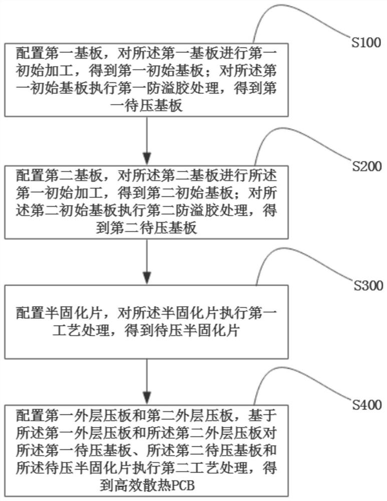
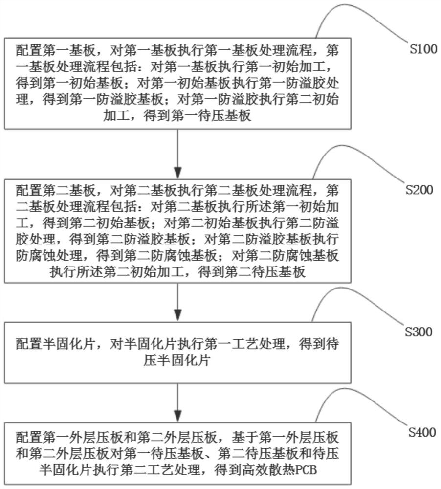
[0069] This embodiment provides a method for manufacturing a high-efficiency heat dissipation PCB, such as Figure 1 to Figure 3 shown, including the following steps:

[0070] This embodiment is applied to the manufacturing process of PCB. When the existing PCB is manufactured, considering the problem of heat dissipation, buried copper block technology and blind groove design will be adopted. The use of these two technologies alone will have a certain adverse effect on the use of PCB. , the manufacturing method of high-efficiency heat dissipation PCB described in this embodiment combines these two technologies, and through the unique process technology involved in this method, the problems existing in the prior art are solved:

[0071] S100. Configure the first substrate, and perform a first substrate processing procedure on the first substrate. The first substrate processing procedure includes: performing a first initial processing on the first substrate to obtain a first ini...

Embodiment 2

[0106] This embodiment provides a manufacturing system for efficient heat dissipation PCB, such as Figure 4 and Figure 5 shown, including:

[0107] The first substrate processing module, the second substrate processing module, the prepreg processing module and the pressing processing module;

[0108] The first substrate processing module is configured to configure the first substrate, and execute the first substrate processing process on the first substrate to obtain the first substrate to be pressed, and the first substrate processing module sends the first substrate to be pressed to the pressing processing module;

[0109] Specifically, the operation of the first substrate processing module includes:

[0110] The first substrate processing module executes the first substrate processing process: the first substrate processing module sets the first size according to the server specification, and performs cutting processing on the first substrate according to the first size...

Embodiment 3

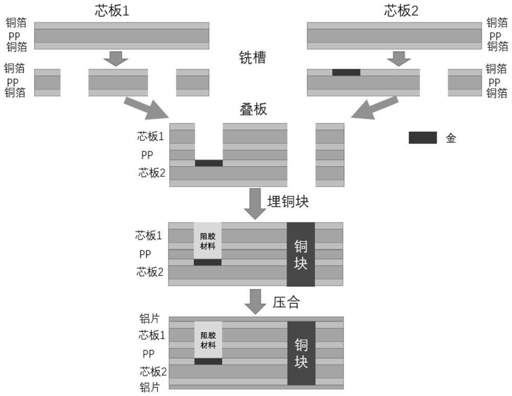
[0125] This embodiment provides a high-efficiency heat dissipation PCB, such as Figure 6 As shown, it includes: a first substrate, a second substrate, a prepreg, a first outer laminate and a second outer laminate;

[0126] The first outer laminate, the first substrate, the prepreg, the second substrate and the second outer laminate are sequentially pressed together; a copper block groove is provided between the first outer laminate and the second outer laminate, and a copper block groove is provided in the copper groove A copper block; a blind groove is provided between the first outer laminate and the second substrate, and a glue-resisting material is arranged in the blind groove; a metal material is plated between the bottom of the glue-resistant material and the bottom of the blind groove;

[0127] In this embodiment, the metal material is gold, the first outer laminate and the second outer laminate are aluminum sheets, the first substrate and the second substrate are both...


PUM


Abstract

The invention discloses a manufacturing method of an efficient heat dissipation PCB. The method comprises the following steps of: configuring a first substrate, and carrying out first initial machining on the first substrate, and obtaining a first initial substrate; performing first glue overflow prevention treatment on the first initial substrate to obtain a first substrate to be pressed; configuring a second substrate, and performing first initial machining on the second substrate to obtain a second initial substrate; and performing second glue overflow prevention treatment on the second initial substrate to obtain a second substrate to be pressed. configuring a prepreg, and performing first process treatment on the prepreg to obtain a prepreg to be pressed; and configuring a first outer laminated board and a second outer laminated board, and performing second process treatment on the first substrate to be pressed, the second substrate to be pressed and the prepreg to be pressed based on the first outer laminated board and the second outer laminated board to obtain the efficient heat dissipation PCB, According to the manufacturing method, the PCB with a heat dissipation function can be manufactured, and it can be ensured that the manufactured PCB has good smoothness, andmeets the high-efficiency heat dissipation requirement.

Description

technical field [0001] The invention relates to the technical field of circuit board manufacturing, in particular to a method, system and PCB for manufacturing a high-efficiency heat dissipation PCB. Background technique [0002] In the prior art, there are two types of PCB (Printed Circuit Board, printed circuit board) with heat dissipation function, one is PCB manufactured by buried copper block technology, this PCB realizes rapid heat dissipation through copper block, but in manufacturing The use of buried copper block technology in the process will make the PCB flatness poor and cause glue flow; the other is a PCB designed with blind slots, which can dissipate heat in a large area through structural forms, but blind slots cannot meet the high efficiency of PCBs Cooling requirements. Contents of the invention [0003] The present invention mainly solves the problems in the prior art that the manufacturing process of the PCB with heat dissipation function is relatively ...

Claims


Application Information

Patent Timeline
Patent Type & Authority Applications(China)
IPC IPC(8): H05K3/46H05K1/02
CPCH05K3/4611H05K1/02H05K1/0203
Inventor 汪亚军
Owner SHANDONG YINGXIN COMP TECH CO LTD
Learn More