
Touch panel, preparation method and display device

A touch panel and bottom surface technology, which is applied in the directions of instruments, computing, and electrical digital data processing, etc., can solve problems such as low production efficiency, long production cycle, and complicated process flow, and achieve simple structure, improved production efficiency, and simplified process. Effect

Pending Publication Date: 2021-08-06
SHANGHAI TIANMA MICRO ELECTRONICS CO LTD
View PDF0 Cites 0 Cited by
  • Summary
  • Abstract
  • Description
  • Claims
  • Application Information

AI Technical Summary

Problems solved by technology

[0003] In order to realize the touch function of the display device, it is usually necessary to introduce touch electrodes into the display device. Different touch electrodes are insulated from each other, and bridges need to be provided between adjacent touch electrodes for connection. Due to the limitation of the process, in practice In the preparation process, multiple metal depositions, photolithography, and etching are required to achieve it, the production cycle is long, the process is complicated, and the production efficiency is low.

Method used


Image

  • Touch panel, preparation method and display device
  • Touch panel, preparation method and display device
  • Touch panel, preparation method and display device

Examples


preparation example Construction

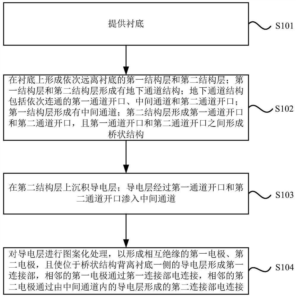
[0034] The embodiment of the present invention provides a method for manufacturing a touch panel, figure 1 It is a schematic flow chart of a method for manufacturing a touch panel provided by an embodiment of the present invention, such as figure 1 As shown, the preparation method of the touch panel of this embodiment includes the following steps:

[0035] S101, providing a substrate.

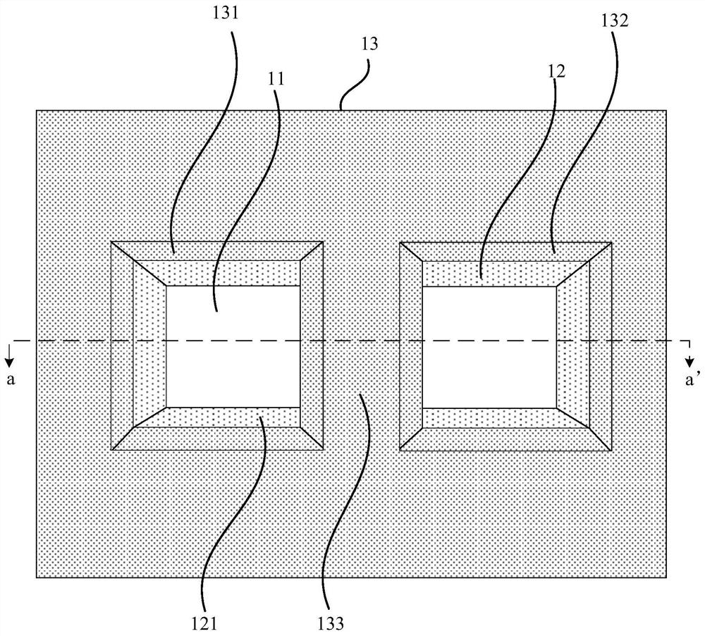
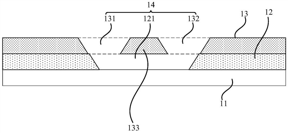
[0036] S102, forming on the substrate a first structural layer and a second structural layer that are sequentially away from the substrate; the first structural layer and the second structural layer are formed with an underground passage structure; the underground passage structure includes sequentially connected first passage openings, middle A channel and a second channel opening; the first structural layer forms a middle channel; the second structural layer forms the first channel opening and the second channel opening, and a bridge structure is formed between the first channel opening and ...


PUM


Abstract

The invention discloses a touch panel, a preparation method and a display device. The preparation method of the touch panel comprises the steps: forming a first structural layer and a second structural layer which are sequentially away from a substrate on the substrate; forming a first channel opening, a middle channel and a second channel opening which are communicated in sequence in the first structural layer and the second structural layer; forming a middle channel in the first structure layer; forming a first channel opening and a second channel opening in the second structure layer, and forming a bridge-shaped structure between the first channel opening and the second channel opening; depositing a conducting layer on the second structure layer, and forming first electrodes and second electrodes which are insulated from each other on the conducting layer, the conducting layer located on the side, away from the substrate, of the bridge-shaped structure forms a first connecting part, and the adjacent first electrodes are electrically connected through the first connecting part, and the adjacent second electrodes are electrically connected through a second connecting part formed by the conductive layer infiltrated into the middle channel. According to the technical scheme provided by the invention, the touch panel which is simple in process and high in production efficiency can be realized.

Description

technical field [0001] The invention relates to the field of display technology, in particular to a touch panel, a manufacturing method, and a display device. Background technique [0002] In recent years, touch technology has been more and more widely used on display devices of various sizes. As a new type of human-computer interaction input display panel, the touch display panel is different from the traditional display, keyboard and mouse input methods. Compared with the touch screen, the input is simpler, more direct and more convenient. [0003] In order to realize the touch function of the display device, it is usually necessary to introduce touch electrodes into the display device. Different touch electrodes are insulated from each other, and bridges need to be provided between adjacent touch electrodes for connection. Due to the limitation of the process, in practice In the preparation process, multiple metal depositions, photolithography, and etching are required t...

Claims


Application Information

Patent Timeline
IPC IPC(8): G06F3/041G06F3/044
CPCG06F3/0412G06F3/0445G06F3/0446G06F2203/04103
Inventor 曹双迎
Owner SHANGHAI TIANMA MICRO ELECTRONICS CO LTD
Features
  • Generate Ideas
  • Intellectual Property
  • Life Sciences
  • Materials
  • Tech Scout
  • Unparalleled Data Quality
  • Higher Quality Content
  • 60% Fewer Hallucinations
Learn More