Pin control circuit and integrated chip

A pin control and control circuit technology, applied in logic circuits, logic circuit coupling/interfaces using field effect transistors, logic circuit interface devices, etc., can solve problems such as low development efficiency, inability to change functions, and inability to realize functions. To achieve the effect of reducing the volume

Pending Publication Date: 2021-08-06
ACTIONS ZHUHAI TECH CO
View PDF0 Cites 0 Cited by
  • Summary
  • Abstract
  • Description
  • Claims
  • Application Information

AI Technical Summary

Problems solved by technology

[0003] In the application development process of the integrated chip, most pins can only realize a single function. Once the pin is occupied, the integrated chip cannot realize the corresponding function.
In order to solve this problem, there is a method of multiplexing pins that use fuses to burn and blow fuses to determine their functions. However, this multiplexing method has the problem that once the function is determined, the function cannot be changed, or it needs to be changed in conjunction with the internal software system. , without the software system can not change the function of the pin
[0004] In order to achieve low power consumption during pin multiplexing, usually the enable pins of an integrated chip can only achieve a single function. If you want to increase the function, you need to add additional pins for communication or control, or use a new chip to replace the original pin. If there is a chip, the layout of the original system circuit board needs to be re-planned, the development efficiency is low, the development cost is high, and the portability is low
[0005] Based on the above situation, the pins of existing integrated chips have a single function, which is not suitable for multi-functional application scenarios.

Method used


Image

  • Pin control circuit and integrated chip
  • Pin control circuit and integrated chip
  • Pin control circuit and integrated chip

Examples


Embodiment Construction

[0026] Embodiments of the present application will be described below in conjunction with the accompanying drawings. It should be understood that the embodiments described here are only used to illustrate and explain the present application, and are not intended to limit the present application.

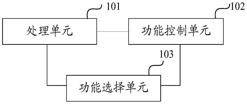
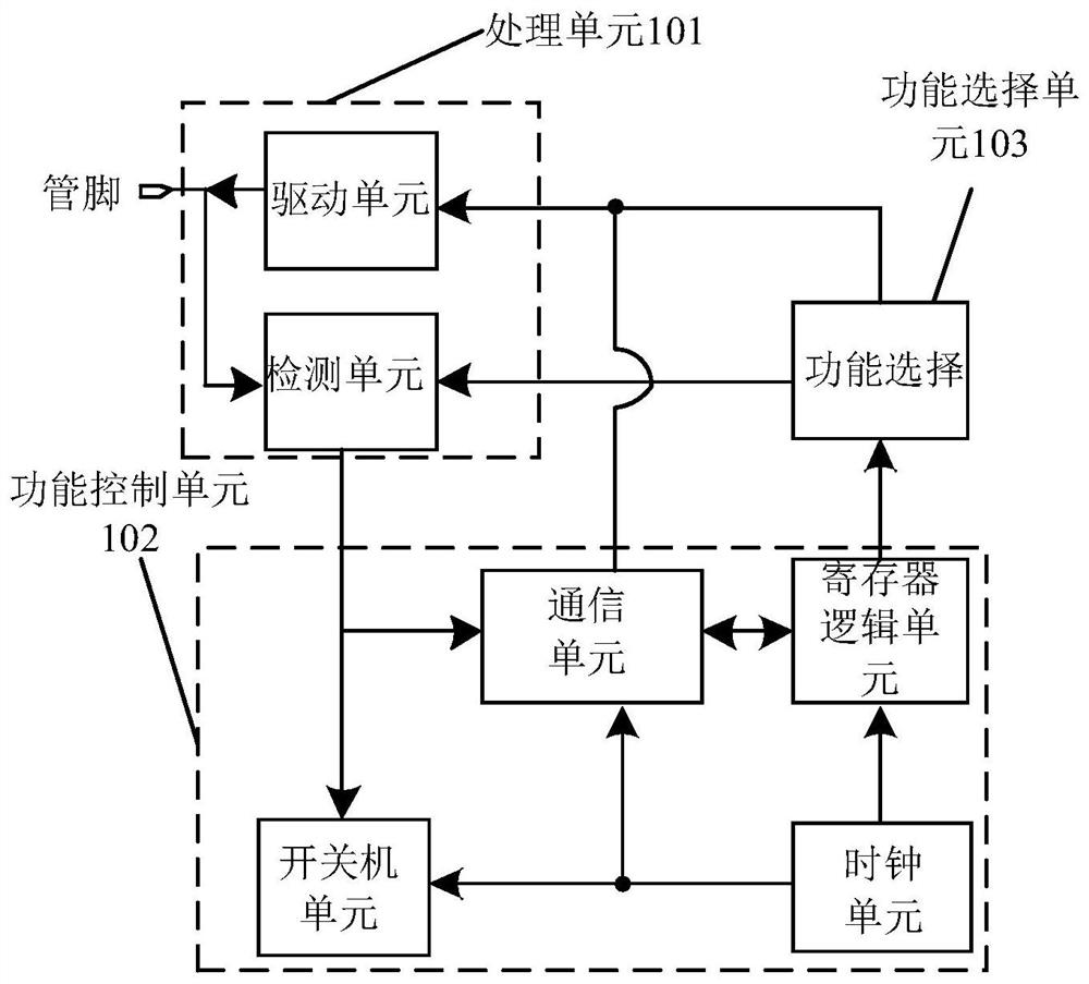
[0027]The specific implementation manners of a pin control circuit and an integrated chip provided by the embodiments of the present invention will be described below in conjunction with the accompanying drawings.

[0028] Most of the current integrated chips have 8-24 pins, and each pin is connected to a fixed external device for receiving signals sent by the external device and realizing corresponding functions according to the received signals. However, in practical applications, for some application scenarios, for example, when the pins used for communication in the integrated chip are occupied, if the external device needs to communicate with the integrated chip at this time, the...


PUM


Abstract

The invention discloses a pin control circuit and an integrated chip, which are used for increasing the functions of pins in the integrated chip and enabling the integrated chip to meet the requirements of a plurality of application scenes. The pin control circuit comprises a processing unit, a function control unit and a function selection unit, wherein the processing unit is connected with the function control unit and the function selection unit, and is used for receiving a signal of the input port and generating a communication signal based on the received signal; the function control unit is connected with the function selection unit and is used for receiving the communication signal and generating a startup and shutdown signal or a data transmission signal according to the communication signal; and the function selection unit is used for receiving the startup and shutdown signal or the data transmission signal, enabling the pin to realize a startup and shutdown function based on the startup and shutdown signal, and enabling the pin to realize a data communication function based on the data transmission signal.

Description

technical field [0001] The invention relates to the technical field of power electronics, in particular to a pin control circuit and an integrated chip. Background technique [0002] In today's electronic technology field, integrated chips are widely used in many scenarios due to their advantages of complete functions and small size, and with the development of science and technology, their achievable functions are also increasing. Connection, external devices are connected to integrated chips through pins to achieve specific functions. [0003] In the application development process of the integrated chip, most pins can only realize a single function. Once the pin is occupied, the integrated chip cannot realize the corresponding function. In order to solve this problem, there is a method of multiplexing pins that use fuses to burn and blow fuses to determine their functions. However, this multiplexing method has the problem that once the function is determined, the functio...

Claims


Application Information

Patent Timeline
Patent Type & Authority Applications(China)
IPC IPC(8): H03K19/0175H03K19/0185H03K17/687
CPCH03K17/687H03K19/017509H03K19/01855
Inventor 王涛冯崧祥曾华丽
Owner ACTIONS ZHUHAI TECH CO
Why Eureka
Try Eureka