A chip flatness detection device and detection method

A detection device and flatness technology, applied in the field of chip flatness detection devices, can solve problems such as low detection efficiency, and achieve the effects of reducing failure rate, reducing loss and improving detection efficiency

Active Publication Date: 2021-09-24
江苏澳芯微电子有限公司
View PDF4 Cites 0 Cited by
  • Summary
  • Abstract
  • Description
  • Claims
  • Application Information

AI Technical Summary

Problems solved by technology

[0004] The purpose of the present invention is to solve the problem of low detection efficiency in the prior art, and propose a chip flatness detection device and detection method

Method used


Image

  • A chip flatness detection device and detection method
  • A chip flatness detection device and detection method
  • A chip flatness detection device and detection method

Examples


Embodiment 1

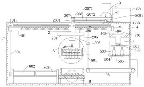
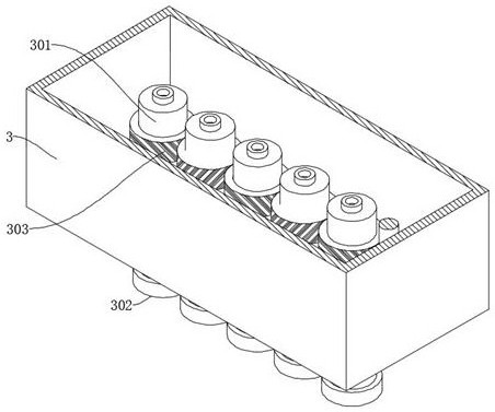
[0036] refer to Figure 1-6, a chip flatness detection device, including a mounting box 1, also includes: a chute 101 opened on the top of the mounting box 1; a pneumatic telescopic rod 2 sliding in the chute 101; Box 3; the connection cylinder 301 connected to the installation box 3 by rotation, wherein the bottom of the connection cylinder 301 extends to the outside of the installation box 3 and is fixedly connected with a suction cup 302, the connection cylinder 301 is provided with multiple groups, and the multiple groups of connection cylinders 301 are all fixed The first gear 303 is connected, and multiple sets of first gears 303 are meshed with each other; the power assembly is arranged in the installation box 3 for driving the connection cylinder 301 to rotate; the detection assembly is arranged in the installation box 1 for detecting the chip .

[0037] Multiple groups of suction cups 302 absorb multiple chips at a time, and send the chips to the top of the detection...

Embodiment 2

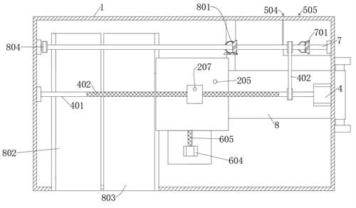
[0039] refer to figure 1 , image 3 with Figure 4 : A chip flatness detection device, which is basically the same as Embodiment 1, and furthermore, the power assembly includes a biaxial motor 304, and the first output shaft of the biaxial motor 304 is fixedly connected with a gear that meshes with the first gear 303 The second gear 305, the top of the installation box 3 is rotatably connected with a connecting shaft 307, the connecting shaft 307 is provided with a safety coupling 3071, and the connecting shaft 307 rotates through the first bevel gear set 306 and the second output shaft of the biaxial motor 304 Connected, the output end of the pneumatic telescopic rod 2 is fixedly connected with the ring gear 202 , and the end of the connecting shaft 307 away from the first bevel gear set 306 is fixedly connected with the third gear 308 meshing with the ring gear 202 .

[0040] Start the biaxial motor 304, the first output shaft of the biaxial motor 304 rotates the first gea...

Embodiment 3

[0042] refer to figure 1 , figure 2 with Figure 5 : A chip flatness detection device, which is basically the same as Embodiment 1, furthermore, the detection assembly includes a base 6, a groove body 602 is slidably connected to the base 6, a detector 603 is provided in the groove body 602, and a detector 603 is arranged on the base 6 A second motor 604 is fixedly connected, the output end of the second motor 604 is fixedly connected with a third reciprocating screw rod 605 , and a second threaded hole corresponding to the third reciprocating screw rod 605 is opened on the tank body 602 .

[0043] Start the tester 603 to detect the flatness of the chip. The tester 603 uses a laser measuring instrument to measure the surface characteristics of the chip by using a laser optical method, and measures the flatness without any contact. The motor 604, the second motor 604 makes the third reciprocating screw mandrel 605 rotate, and the third reciprocating screw mandrel 605 makes t...


PUM


Abstract

The invention discloses a chip flatness detection device and a detection method, belonging to the technical field of chip detection equipment. A chip flatness detection device, including a mounting box, also includes: a chute set on the top of the mounting box; a pneumatic telescopic rod sliding in the chute; a mounting box connected to the output end of the pneumatic telescopic rod; The connecting cylinder on the top, wherein, the bottom of the connecting cylinder extends to the outside of the installation box and is fixedly connected with a suction cup. The connecting cylinder is provided with multiple sets, and the multiple sets of connecting cylinders are fixedly connected with first gears, and the multiple sets of first gears mesh with each other; The assembly is arranged in the installation box and is used to drive the connection cylinder to rotate; the detection assembly is arranged in the installation box and is used to detect the chip; the invention adjusts the relative position of the chip and the detector by making the connection shaft and the installation box rotatable. Surface, so that the bottom surface and side wall of multiple groups of chips can be tested for flatness at the same time, thereby improving the detection efficiency.

Description

technical field [0001] The invention relates to the technical field of chip testing equipment, in particular to a chip flatness testing device and testing method. Background technique [0002] A semiconductor chip is a semiconductor device that is etched and wired on a semiconductor sheet to achieve a certain function; not only a silicon chip, but also common semiconductor materials such as gallium arsenide and germanium; after the semiconductor chip is produced, Workers are required to test the thickness of the semiconductor chip and the flatness of the pins after production, so as to facilitate the subsequent use of the semiconductor chip. [0003] At present, when testing a specific semiconductor chip, workers need to use calipers to detect and evaluate it, so it is not convenient to test a large number of semiconductor chips. When testing by laser, it is necessary to use a robot to transport the chip. The bottom and four sides of the chip need to be tested for flatness,...

Claims


Application Information

Patent Timeline
Patent Type & Authority Patents(China)
IPC IPC(8): G01B11/30B65G47/91B66C19/00B66C1/02B66C5/02B66C9/10B66C9/14B66C13/08
CPCB65G47/91B66C1/025B66C1/0262B66C5/02B66C9/10B66C9/14B66C13/085B66C19/00G01B11/30
Inventor 王印玺
Owner 江苏澳芯微电子有限公司
Why Eureka
Try Eureka