High-gain low-stress photovoltaic multi-level inverter and control method thereof
A multi-level inverter, low-stress technology, applied in photovoltaic power generation, electrical components, AC power input conversion to DC power output, etc., can solve the problem of voltage reduction at the maximum power point, DC capacitor voltage equalization, and no boost functions and other issues to achieve the effect of reducing control complexity and increasing output level
- Summary
- Abstract
- Description
- Claims
- Application Information
AI Technical Summary
Problems solved by technology
Method used
Image
Examples
Embodiment 1
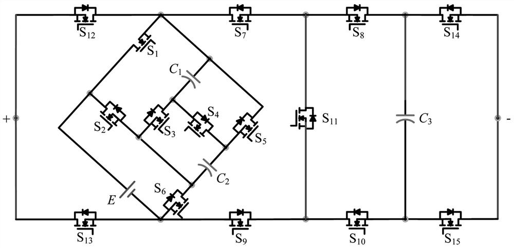
[0051] Such as figure 1 As shown, a high-gain low-stress photovoltaic multilevel inverter includes a boost unit, an I-shaped switch structure, and an independent capacitor C 3 and two half-bridge structures; the inverter in this embodiment consists of a boost unit and an independent capacitor C 3 It is formed by connecting the I-shaped switch structure, and using two half-bridge structures instead of the H-bridge to convert the polarity of the output level.
[0052] The boost unit includes a photovoltaic DC power supply E, an electrolytic capacitor C 1 , electrolytic capacitor C 2 , switch tube S 2 , switch tube S 3 , switch tube S 4 , switch tube S 5 , switch tube S 6 and switch S without reverse diode 1 ; The switch tube S 1 The input terminal and the switch tube S 2 The input terminal of the photovoltaic DC power supply E is connected to the positive pole; the switch tube S 1 output terminal with electrolytic capacitor C 1 Anode of the switch tube S 5 The input...
Embodiment 2
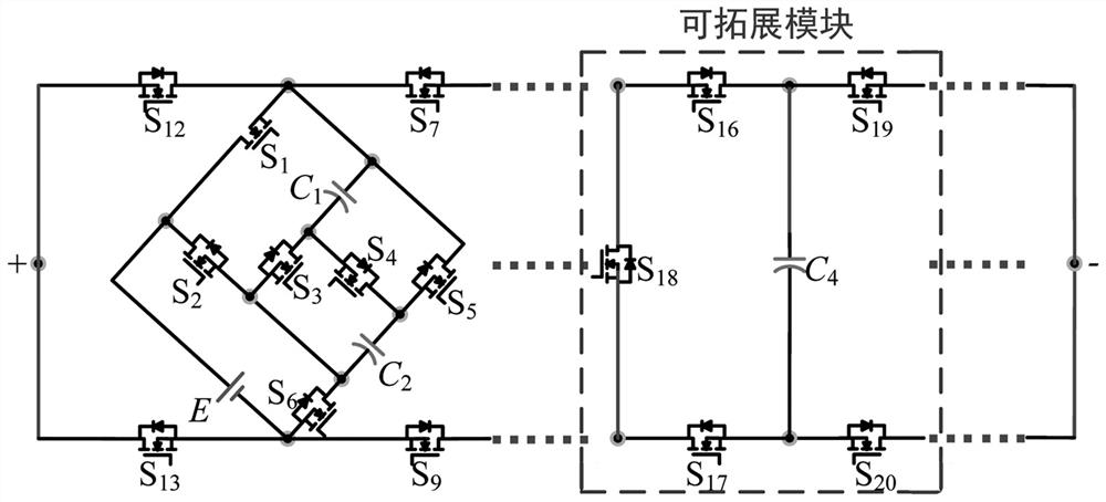
[0061] Such as figure 2 As shown, this embodiment provides a scalable high-gain low-stress photovoltaic multilevel inverter, including the high-gain low-stress photovoltaic multilevel inverter described in Embodiment 1 and an expandable module;
[0062] The expandable module includes a switch tube S 16 , switch tube S 17 , switch tube S 18 , switch tube S 19 , switch tube S 20 and electrolytic capacitor C 4 ; The switch tube S 16 The input terminal and the switch tube S 19 The input terminal, electrolytic capacitor C 4 The anode is connected; the switching tube S 16 The output terminal of the switch tube S 18 The input terminal is connected; the switch tube S 17 The input terminal and the switch tube S 18 The output terminals are connected; the switch tube S 17 The output terminal of the switch tube S 20 The output terminal, the electrolytic capacitor C 4 connected to the cathode.
[0063]The boost unit charges all expandable modules at the same time, and each ...
Embodiment 3
[0065] This embodiment provides a control method for a high-gain and low-stress photovoltaic multilevel inverter:
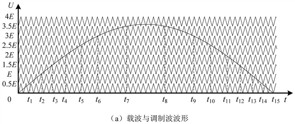
[0066] Generate a driving signal, and control the high-gain and low-stress photovoltaic multilevel inverter described in Embodiment 1 to work in 17 working states and output 17 levels through the driving signal, and the high-gain and low-stress photovoltaic multi-level inverter Level inverter output 4 times voltage gain.
[0067] Specifically, the modulation principle shown in Figure 3(a)-3(d) adopts carrier stacking pulse width modulation technology, using 16 channels of triangular carriers with the same amplitude and frequency to be stacked in sequence, and 1 channel of sine modulation wave After comparison, the obtained 16 channels of original pulse waveforms are logically combined to obtain a gate pulse drive signal for driving the switching tube on and off. The inverter has a large number of output levels, and the principle of the modulation strategy is rep...
PUM
 Abstract
Description
Claims
Application Information


