Integrated memory cell and memory array

A technology of storage unit and storage transistor, which is applied in the field of memory, can solve the problem of unreliable data transfer, achieve high reliability, reduce production cost, and save the overall area

Active Publication Date: 2021-08-17
上海亿存芯半导体有限公司
View PDF12 Cites 0 Cited by
  • Summary
  • Abstract
  • Description
  • Claims
  • Application Information

AI Technical Summary

Problems solved by technology

[0005] The object of the present invention is to provide an integrated storage unit and storage array to

Method used


Image

  • Integrated memory cell and memory array
  • Integrated memory cell and memory array
  • Integrated memory cell and memory array

Examples


Example Embodiment

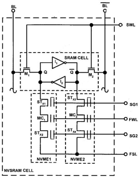
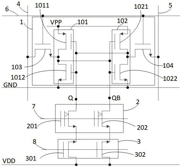
[0041] As a preferred embodiment of the present invention, the first inverter 101 includes a first PMOS tube 1011 and a first NMOS tube 1012, the first PMOS tube 1011 source connection programming erase voltage end VPP, The drain of the first PMOS tube 1011 is connected to the drain of the first NMOS tube 1012, and the gate of the first PMOS tube 1011 connects the gate of the first NMOS tube 1012, the first NMOS tube 1012. The source grounded. The second inverter 102 includes a second PMOS tube 1021 and a second NMOS tube 1022, the source of the second PMOS tube 1021 connects the programming erase voltage end VPP, the leakage of the second PMOS tube 1021 The drain of the second NMOS tube 1022 is electrically connected, the gate of the second PMOS tube 1021 connects the gate of the second NMOS tube 1022, the source of the second NMOS tube 1022, and the first The gate of the NMOS tube 1012 is connected to the first input of the non-volatile memory unit 2, and the gate of the second ...


PUM


Abstract

The invention provides an integrated storage unit. The storage unit comprises a static random access storage unit; a non-volatile memory cell including a first memory transistor and a second memory transistor; a gate unit which comprises a first gate NMOS tube and a second gate NMOS tube, wherein the first gate NMOS tube and the second gate NMOS tube are used for loading data in the nonvolatile memory unit to the static random access memory unit, and the first gate NMOS tube and the second gate NMOS tube are used as control tubes of the nonvolatile memory unit; therefore, the total area of the memory is saved, the memory is compatible with erasing, programming and reading operations of the non-volatile memory unit, and the reliability of data transfer between the static random access memory unit and the non-volatile memory unit is high. The invention further provides a storage array. The storage array comprises at least one integrated storage unit.

Description

technical field [0001] The invention relates to the technical field of memory, in particular to an integrated memory unit and a memory array. Background technique [0002] Static Random-Access Memory (SRAM) is a semiconductor storage device that uses various mechanisms to store state. For example, an SRAM may store a logic low or "0" in one configuration and a logic high or "1" in another configuration. SRAM can be used in computer design because of its relatively low power consumption, speed, and ease of operation. One application of SRAM is as configuration memory for Field Programmable Gate Arrays (FPGAs). SRAM has a faster read and write speed than other memories, but the stored data will be lost when the power is turned off. However, if the non-volatile memory is combined with the static random access memory, each storage unit is connected with more control switch tubes, the memory chip area is large, the structure is complex, and the cost is high. The data between t...

Claims


Application Information

Patent Timeline
IPC IPC(8): G11C11/409H01L27/11
CPCG11C11/409H10B10/00
Inventor 袁庆鹏蔡晓波张思萌张新龙
Owner 上海亿存芯半导体有限公司
Why Eureka
Try Eureka