Bonding equipment and bonding process for chip processing

A bonding and chip technology, which is applied in metal processing equipment, welding equipment, optical mechanical equipment, etc., can solve the problems of shaking of the bonding base, inconvenient replacement, bonding offset, etc., and achieve the effect of improving stability

Active Publication Date: 2021-08-20
芯创(天门)电子科技有限公司
View PDF8 Cites 0 Cited by
  • Summary
  • Abstract
  • Description
  • Claims
  • Application Information

AI Technical Summary

Problems solved by technology

[0005] Aiming at the deficiencies of the existing technology, the present invention provides a bonding equipment for chip processing, which has the advantages of safe bonding and stable bonding, and solves the problem that residual heat still exists and is not convenient for direct replacement. Due to the long bonding process, There is a problem that the bonding base shakes, causing the bonding to shift

Method used


Image

  • Bonding equipment and bonding process for chip processing
  • Bonding equipment and bonding process for chip processing
  • Bonding equipment and bonding process for chip processing

Examples


Embodiment Construction

[0033] The following will clearly and completely describe the technical solutions in the embodiments of the present invention with reference to the accompanying drawings in the embodiments of the present invention. Obviously, the described embodiments are only some, not all, embodiments of the present invention. Based on the embodiments of the present invention, all other embodiments obtained by persons of ordinary skill in the art without making creative efforts belong to the protection scope of the present invention.

[0034] As introduced in the background, there are deficiencies in the prior art. In order to solve the above technical problems, the present application proposes a bonding device for chip processing.

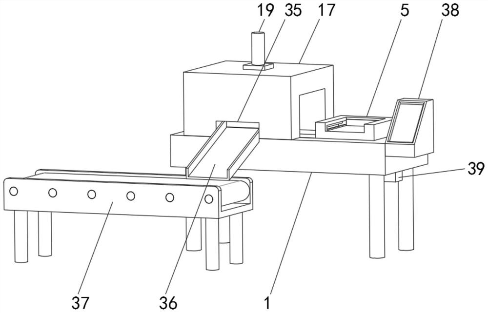
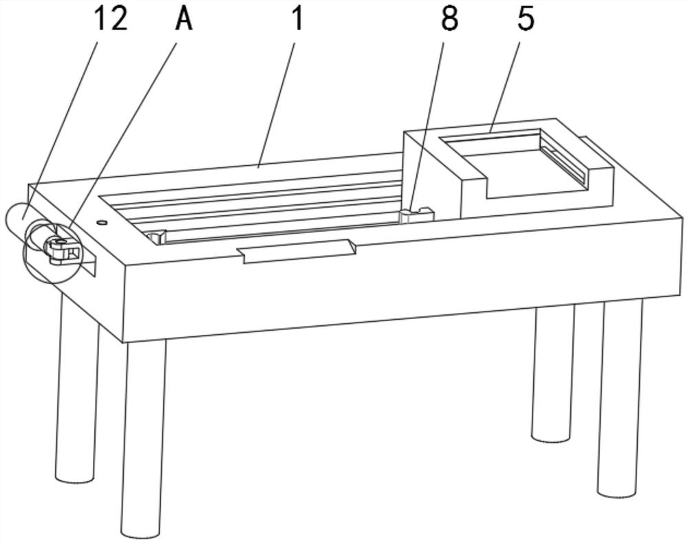
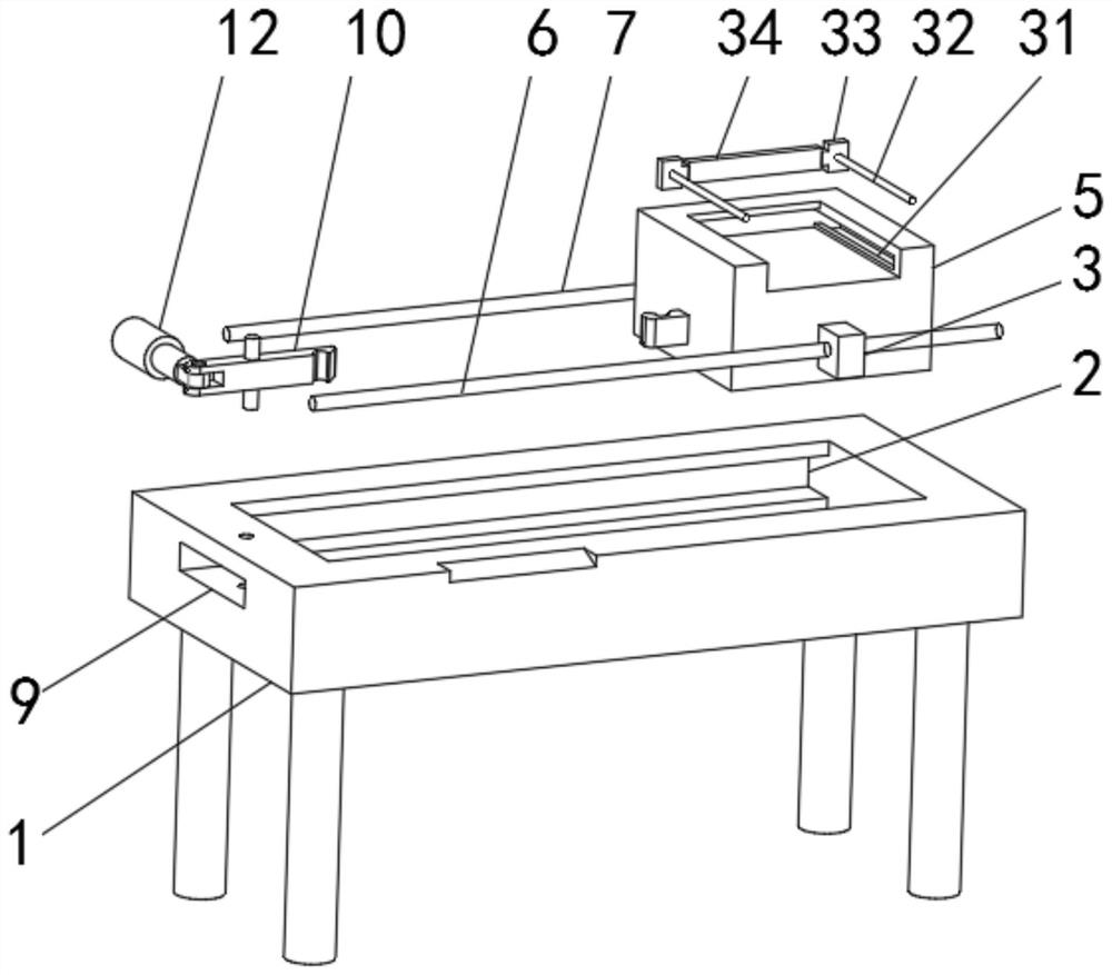
[0035] see Figure 1-7, a bonding device for chip processing, including a mounting table 1, both sides of the inner wall of the mounting table 1 are provided with chute 2, and the sliding grooves 2 on both sides of the mounting table 1 are respectively slidably ...


PUM


Abstract

The invention relates to the technical field of chip processing, and discloses bonding equipment for chip processing and a bonding process. The bonding equipment comprises a mounting table, the two sides of the inner wall of the mounting table are both provided with sliding grooves, the interiors of the sliding grooves in the two sides of the mounting table are slidably connected with a limiting block and an electric sliding block respectively, and the limiting block and the electric sliding block are fixedly connected to the middles of the two sides of a pressing table respectively. The pressing table is driven by power of an electric sliding rail and the electric sliding block to move under the matching action of the limiting block and the sliding groove, the pressing table slides into a pressing furnace, then a clamping plate is extruded through a clamping hook, the clamping plate rotates in a clamping groove, a reset spring in an insulating cylinder is compressed at the moment, and when the clamping hook is clamped into the clamping plate, the clamping plate is rapidly reset under the elastic force action of the reset spring so that the clamping hook and the clamping plate are clamped with each other, the pressing table is further fixed, the pressing table is further ensured not to shake in the pressing process, and the condition of bonding deviation caused by shaking is avoided.

Description

technical field [0001] The invention relates to the technical field of chip processing, in particular to a bonding device and a bonding process for chip processing. Background technique [0002] Chips made of silicon have amazing computing power. The development of science and technology is constantly promoting the development of semiconductors. The development of technologies such as automation and computers has reduced the cost of high-tech products such as silicon chips (integrated circuits) to a very low level. This makes silicon wafers widely used in aerospace, industry, agriculture and national defense. Silicon wafer bonding technology refers to the method of tightly combining silicon wafers with silicon wafers, silicon wafers with glass or other materials through chemical and physical actions. Silicon wafer bonding is often combined with surface silicon processing and bulk silicon processing, and is used in the processing technology of MEMS. Common silicon wafer bo...

Claims


Application Information

Patent Timeline
IPC IPC(8): H01L21/603B81C3/00
CPCH01L24/75H01L24/76H01L24/81H01L24/82B81C3/001B81C3/004H01L2224/75313H01L2224/75705H01L2224/76313H01L2224/76703H01L2224/81121H01L2224/8118H01L2224/82121H01L2224/8218H01L2224/82201
Inventor 杨汉林代磊
Owner 芯创(天门)电子科技有限公司
Why Eureka
Try Eureka