PCB tin soldering equipment and PCB machining technology

A PCB circuit board, circuit board technology, applied in welding equipment, metal processing, metal processing equipment and other directions, can solve problems such as burns, pads falling off, accidental contact with hot melt adhesive, etc., to facilitate welding, prevent skin burns, welding Process clear effect

Active Publication Date: 2021-08-24
浙江航都科技有限公司
View PDF8 Cites 2 Cited by
  • Summary
  • Abstract
  • Description
  • Claims
  • Application Information

AI Technical Summary

Problems solved by technology

[0005] Aiming at the deficiencies of the prior art, the present invention provides a soldering equipment for PCB circuit boards, which has the advantages of cooling pads and preventing operators from being scalded by hot melt adhesives, and solves the problem of solder pads falling off and operators accidentally touching hot melt adhesives. The problem

Method used


Image

  • PCB tin soldering equipment and PCB machining technology
  • PCB tin soldering equipment and PCB machining technology
  • PCB tin soldering equipment and PCB machining technology

Examples


Embodiment Construction

[0033]The following will clearly and completely describe the technical solutions in the embodiments of the present invention with reference to the accompanying drawings in the embodiments of the present invention. Obviously, the described embodiments are only some, not all, embodiments of the present invention. Based on the embodiments of the present invention, all other embodiments obtained by persons of ordinary skill in the art without making creative efforts belong to the protection scope of the present invention.

[0034] As introduced in the background technology, there are deficiencies in the prior art. In order to solve the above technical problems, the application proposes a PCB circuit board soldering equipment

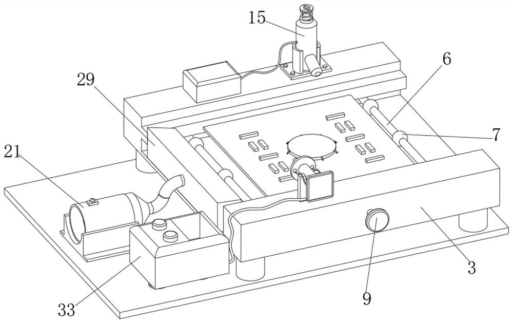
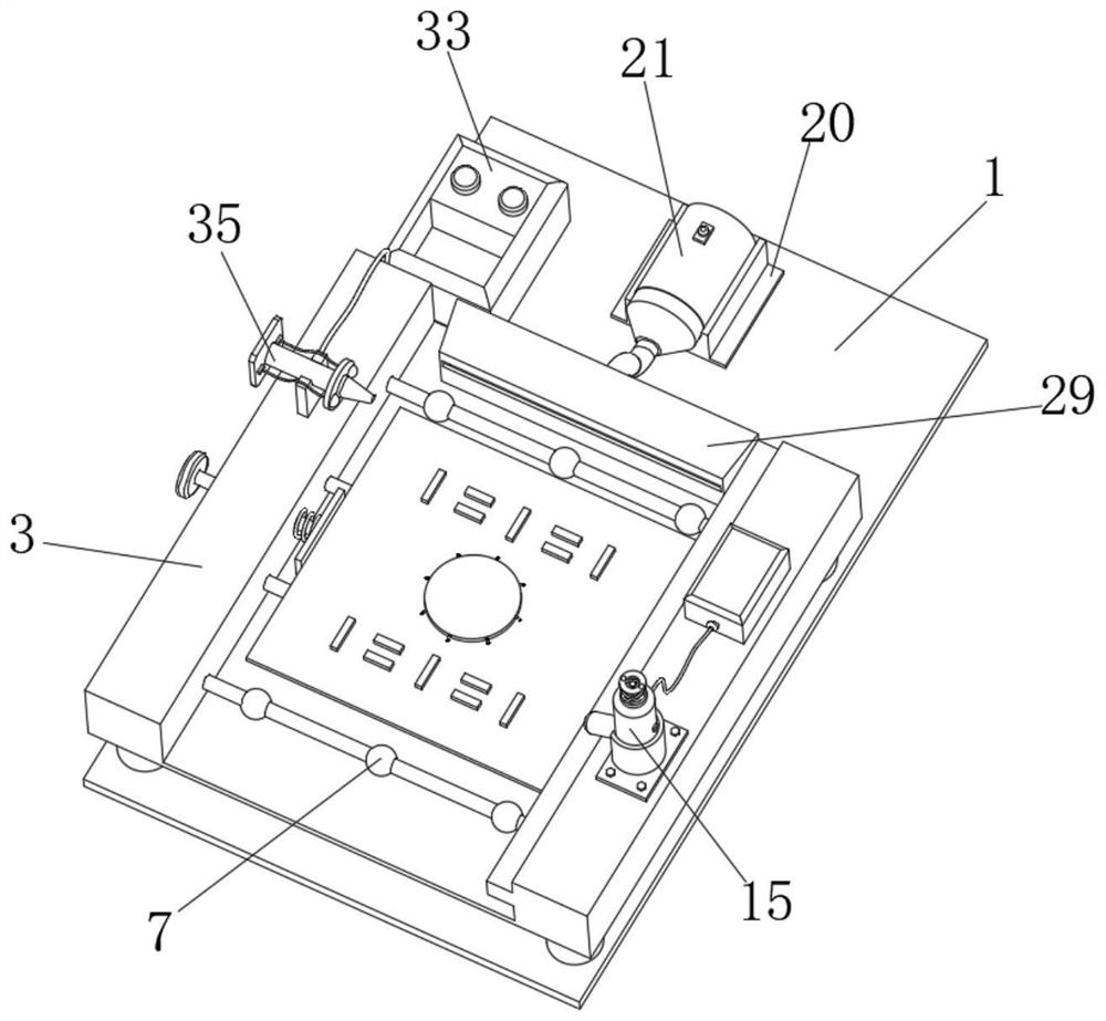
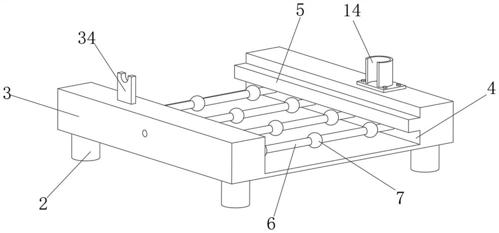
[0035] In a typical implementation of the present application, such as Figure 1-8 As shown, a PCB circuit board soldering equipment includes a base 1, the top of the base 1 is fixedly connected with four support fixed columns 2, and the tops of the four sup...


PUM


Abstract

The invention relates to the technical field of circuit board tin soldering equipment, and discloses PCB tin soldering equipment and a PCB machining technology. A hot melting gun is aligned with a circuit board to extrude a hot melt adhesive, a sliding hemisphere is in contact with the circuit board, an extrusion spring generates elastic deformation, a top ring is pressed to move towards a fixed bottom ring, the skin of a user can be prevented from being scalded when the hot melt adhesive is pressed, a driving motor is started, the output end of the driving motor drives an input shaft to rotate through a coupler, the input shaft enables a fan to rotate, the fan rotates at a high speed to generate certain air volume, air is blown into a cooling box through a cooling pipe and is blown to the circuit board through rectangular air outlet holes, a bonding pad can be cooled, the phenomenon that the bonding pad falls off caused by thermal expansion and cold contraction due to the fact that a metal plate of the bonding pad generates large temperature difference is avoided, the circuit board can slide in an operation table through the arrangement of multiple balls, and therefore the circuit board can be conveniently taken out of the operation table, and time and labor are saved.

Description

technical field [0001] The invention relates to the technical field of circuit board soldering equipment, in particular to a PCB circuit board soldering equipment and a PCB circuit board processing technology. Background technique [0002] Circuit boards, circuit boards, PCB boards, soldering technology In recent years, in the development of electronics industry technology, it can be noticed that an obvious trend is reflow soldering technology. In principle, traditional plug-in parts can also be used in reflow soldering process, which is commonly referred to as through-hole reflow soldering. The advantage is that it is possible to complete all solder joints at the same time, which minimizes production costs. However, temperature-sensitive components limit the application of reflow soldering, whether it is a plug-in or SMD. Then people turn their attention to selective soldering. Selective soldering can be used after reflow soldering in most applications and will be an econo...

Claims


Application Information

Patent Timeline
Patent Type & Authority Applications(China)
IPC IPC(8): B23K3/00B23K3/08H05K3/34B23K101/42
CPCB23K3/00B23K3/08H05K3/3421H05K3/3447B23K2101/42
Inventor 徐琳
Owner 浙江航都科技有限公司
Why Eureka
Try Eureka