Graphical photosensitive resin coating and manufacturing method thereof, circuit structure and capacitive touch screen
A technology of photosensitive resin and production method, which is applied in the direction of photosensitive materials used in optomechanical equipment, electrical digital data processing, instruments, etc., and can solve problems such as poor refractive index, large opening area, and large photosensitive resin coating area , to achieve the effect of saving area, reducing area and preventing the appearance from being affected
- Summary
- Abstract
- Description
- Claims
- Application Information
AI Technical Summary
Problems solved by technology
Method used
Image
Examples
Embodiment 1
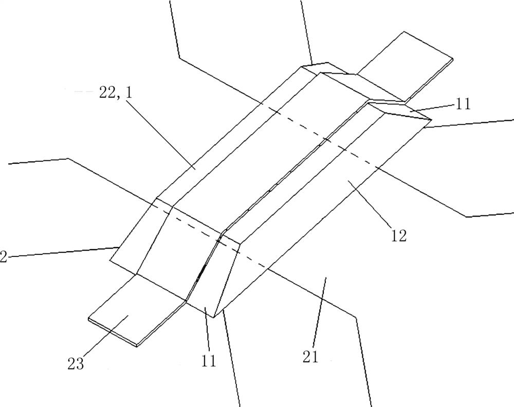
[0035] Such as Figure 1-Figure 6 As shown, this patterned photosensitive resin coating 1 is arranged on a surface of the substrate 0, and a first axis and a second axis orthogonal to each other are defined based on the surface of the substrate 0; along the first axis, the photosensitive resin coating Layer 1 has at least one first edge slope 11, the slope angle of the first edge slope 11 is smaller than the slope angle of other edge slopes; along the second axis, the photosensitive resin layer 1 has at least one second edge slope 12, the second edge slope The slope angle of 12 is greater than the slope angles of other edge slopes; the photosensitive resin coating 1 is coated with a negative photosensitive resin and exposed and cured by an anisotropic ultraviolet light source 5, and the anisotropic ultraviolet light source 5 is formed at the first edge slope 11 The light scattering angle is the first light scattering angle 501, the light scattering angle of the anisotropic ult...
Embodiment 2
[0047] refer to Figure 7 , in the case that other parts are the same as in Embodiment 1, the difference is that in this embodiment, the anisotropic ultraviolet light source 5' includes an ultraviolet lamp 51' and a plurality of U-shaped baffles 52', and each U-shaped The baffles 52' are stacked in sequence to form a baffle group with a strip-shaped cavity, and the ultraviolet lamp 51' is located in the strip-shaped cavity. The graphic mask 4 is directly attached to the substrate 0 . During operation, the ultraviolet light emitted by the ultraviolet lamp tube 51' passes through the gap between the lower edges of each U-shaped block 52', and then irradiates towards the photosensitive resin coating 1 on the substrate 0 through the non-shading part of the pattern mask plate 4. , due to being blocked by each U-shaped baffle 52', the first light scattering angle 501 of the anisotropic ultraviolet light source 5' along the first axis can be larger than other light scattering angles...
Embodiment 3
[0049] refer to Figure 8 , in the case that other parts are all the same as in Embodiment 1, the difference is that in this embodiment, the upper surface of the photosensitive resin coating 1 is provided with a square hole 10 penetrating up and down, and the cross-sectional area of the square hole 10 is from Tapered from top to bottom, the inner wall of the square hole 10 has two first edge slopes 11 opposite to each other along the first axis and two second edge slopes 12 opposite to each other along the second axis.
[0050] The circuit structure 2' provided in this embodiment includes a first conductive layer 21', an insulating layer 22' and a second conductive layer 23' sequentially arranged on the substrate 0 from inside to outside, and the insulating layer 22' is the patterned Photosensitive resin coating 1, the first conductive layer 21' extends to the bottom of the square hole 10, and the second conductive layer 23' extends from a first edge slope 11 of the insulati...
PUM
| Property | Measurement | Unit |
|---|---|---|
| angle | aaaaa | aaaaa |
Abstract
Description
Claims
Application Information


