Supercharge Your Innovation With Domain-Expert AI Agents!

Shielded gate field effect transistor and method of forming the same

A field-effect transistor and shielding gate technology, which is applied in semiconductor devices, semiconductor/solid-state device manufacturing, electrical components, etc., can solve problems such as adverse effects, achieve the effects of ensuring filling performance, avoiding poor patterning accuracy, and simplifying settings

Active Publication Date: 2022-08-09
SEMICON MFG ELECTRONICS (SHAOXING) CORP
View PDF6 Cites 0 Cited by
  • Summary
  • Abstract
  • Description
  • Claims
  • Application Information

AI Technical Summary

Problems solved by technology

[0010] The object of the present invention is to provide a method for forming a shielded gate field effect transistor to solve the adverse effects caused by the grinding process in the existing forming method

Method used


Image

  • Shielded gate field effect transistor and method of forming the same
  • Shielded gate field effect transistor and method of forming the same
  • Shielded gate field effect transistor and method of forming the same

Examples


Embodiment Construction
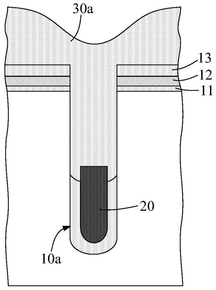
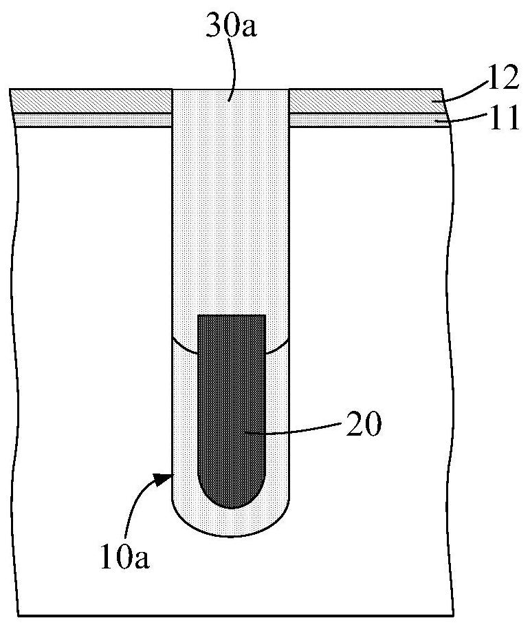
[0030] The core idea of ​​the present invention is to provide a method for forming a shielded gate field effect transistor. Compared with the existing preparation method, the grinding process can be avoided during the preparation process of the isolation layer, thereby avoiding the problems caused by the grinding process. adverse effects.

[0031] For details, please refer to image 3 As shown, the method for forming the shielded gate field effect transistor includes the following steps.

[0032] Step S100, a substrate is provided, a trench is formed in the substrate, and a shield electrode is formed in the trench.

[0033] Step S200, forming an isolation material layer in the trench, the top surface of the isolation material layer in the trench is not lower than a predetermined height, and the isolation material layer does not fill the trench.

[0034] Step S300 , forming a sacrificial material layer on the isolation material layer and filling the trench, the material of th...


PUM

PropertyMeasurementUnit
thicknessaaaaaaaaaa

Abstract

The present invention provides a shielded gate field effect transistor and a method for forming the same. When preparing the isolation layer, a sacrificial material layer with fluidity under predetermined conditions is used to achieve the flatness of the top surface of the film layer before etching, and the isolation layer with a flat surface is formed based on the subsequent etching process. That is, the formation method provided by the present invention may not use the grinding process when preparing the isolation layer, thereby effectively avoiding the defects caused by the grinding process, and helping to reduce the size of the device.

Description

technical field [0001] The present invention relates to the technical field of semiconductors, in particular to a shielded gate field effect transistor and a method for forming the same. Background technique [0002] Shielded gate field effect transistor (Shielded Gate Trench, SGT), because of its low gate-drain capacitance Cgd, low on-resistance, and high withstand voltage performance, which is more conducive to the flexible application of semiconductor integrated circuits. Specifically, in the shielded gate field effect transistor, by arranging the shielding electrode below the gate electrode, the gate-to-drain capacitance can be greatly reduced, and the drift region of the shielded gate field effect transistor also has higher impurity carriers concentration, which can provide additional benefits to the breakdown voltage of the device, and correspondingly lower on-resistance. [0003] Compared with other trench field effect transistors, although the shielded gate field ef...

Claims


Application Information

Patent Timeline
Patent Type & Authority Patents(China)
IPC IPC(8): H01L21/336H01L21/28H01L29/78H01L29/423
CPCH01L29/66734H01L21/28114H01L29/7813H01L29/4236
Inventor 李艳旭
Owner SEMICON MFG ELECTRONICS (SHAOXING) CORP
Features
  • R&D
  • Intellectual Property
  • Life Sciences
  • Materials
  • Tech Scout
  • Unparalleled Data Quality
  • Higher Quality Content
  • 60% Fewer Hallucinations
Learn More