Three-dimensional semiconductor memory devices

A memory and semiconductor technology, applied in the direction of semiconductor devices, semiconductor/solid-state device components, electric solid-state devices, etc., can solve the problems of increasing the integration of two-dimensional or planar semiconductor devices, and being extremely expensive

Pending Publication Date: 2021-08-27
SAMSUNG ELECTRONICS CO LTD
View PDF1 Cites 0 Cited by
  • Summary
  • Abstract
  • Description
  • Claims
  • Application Information

AI Technical Summary

Problems solved by technology

However, increasing pattern fineness requires expensive (and potentially extremely expensive or too expensive) processing equipment, which poses a practical limit to increasing the integration of two-dimensional or planar semiconductor devices

Method used


Image

  • Three-dimensional semiconductor memory devices
  • Three-dimensional semiconductor memory devices
  • Three-dimensional semiconductor memory devices

Examples


Embodiment Construction

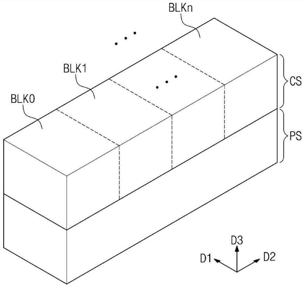
[0027] figure 1 is a schematic perspective view illustrating a three-dimensional semiconductor memory device according to some embodiments of the inventive concept.

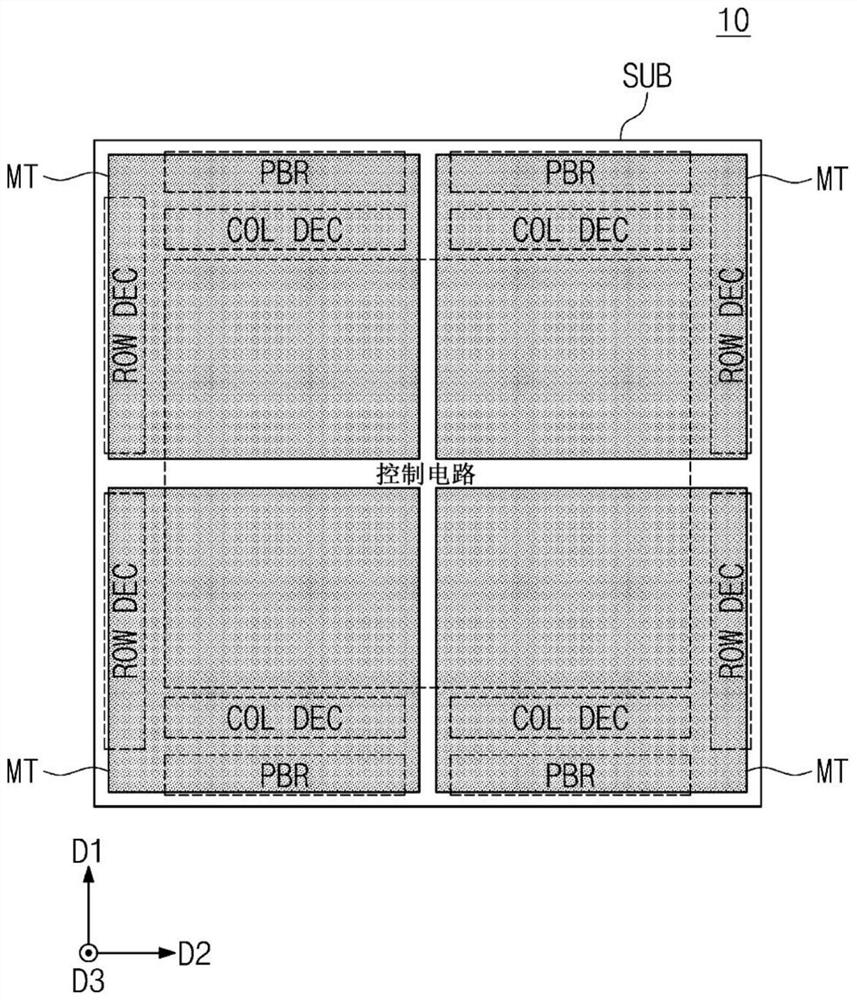
[0028] refer to figure 1 A three-dimensional semiconductor memory device according to some embodiments of the inventive concepts may include a peripheral circuit structure PS, a cell array structure CS on the peripheral circuit structure PS, and through contacts ( not shown). The cell array structure CS may overlap the peripheral circuit structure PS when viewed in a plan view.

[0029] In some embodiments, the peripheral circuit structure PS may include row and column decoders, page buffers, control circuits, and peripheral logic circuits. Components of the peripheral circuit structure PS (eg, peripheral logic circuits) may be integrated on a semiconductor substrate.

[0030] The cell array structure CS may include a cell array including a plurality of memory cells three-dimensionally arranged on a semicondu...


PUM


Abstract

A semiconductor device includes a substrate including a lower horizontal layer and an upper horizontal layer and having a cell array region and a connection region; an electrode structure including electrodes, which are stacked above the substrate, and which extend from the cell array region to the connection region; a vertical channel structure on the cell array region that penetrates the electrode structure and is connected to the substrate; and a separation structure on the connection region that penetrates the electrode structure. The lower horizontal layer has a first top surface in contact with a first portion of the separation structure, and a second top surface in contact with a second portion of the separation structure, and an inflection point at which a height of the lower horizontal layer is abruptly changed between the first top surface and the second top surface.

Description

[0001] Cross References to Related Applications [0002] This application claims priority to Korean Patent Application No. 10-2020-0024333 filed with the Korean Intellectual Property Office on February 27, 2020, the entire contents of which are incorporated herein by reference. technical field [0003] The present disclosure relates to semiconductor devices, and in particular, to a three-dimensional semiconductor memory device with improved reliability. Background technique [0004] There is an ongoing and growing consumer demand to achieve higher performance, lower cost electronic devices. These demands can be met in part by increasing the integration degree of semiconductor devices used in electronic devices, since integration is an important factor in determining product prices in terms of semiconductor devices. For two-dimensional or planar semiconductor devices, integration depends primarily on the area occupied by a unit memory cell, so this integration can be greatly...

Claims


Application Information

Patent Timeline
Patent Type & Authority Applications(China)
IPC IPC(8): H01L27/11524H01L27/11556H01L27/1157H01L27/11582H10B41/35H10B43/30H10B41/10H10B41/27H10B41/40H10B43/10H10B43/27H10B43/35H10B43/40H10B43/50
CPCH10B41/35H10B41/27H10B43/35H10B43/27H10B43/10H10B43/40H01L29/792H01L29/66833H10B43/30H10B43/50H01L23/528H10B41/10H10B41/40
Inventor 郑圣勋李秉一李俊熙
Owner SAMSUNG ELECTRONICS CO LTD
Why Eureka
Try Eureka