
Multi-chip packaging structure and packaging method

A multi-chip packaging and packaging method technology, applied in the direction of semiconductor/solid-state device components, semiconductor devices, electrical components, etc., can solve problems such as affecting product reliability, unfilled space, touch, etc. Risk, relative height reduction, size reduction effect

Pending Publication Date: 2021-08-31
通富微电科技(南通)有限公司
View PDF0 Cites 1 Cited by
  • Summary
  • Abstract
  • Description
  • Claims
  • Application Information

AI Technical Summary

Problems solved by technology

This combined structure has the following disadvantages: (1) The front-loading chip is fixed on the substrate by the mounting adhesive, and since the mounting adhesive will overflow, it is necessary to control the distance between the bonding wire and the chip, the passive components and the conductive bumps. The block will be moved out correspondingly, which increases the plane size of the package structure; (2) Based on the limitation of the current flip-chip welding process, there is a risk of touching the bonding wire of the front-mounted chip when the flip-chip is mounted. The height of the bump and the process capability of the flip chip welding process require more input costs; (3) When the area between the flip chip and the front chip is filled with mold flow, there is a risk of insufficient space (height). , affecting product reliability

Method used


Image

  • Multi-chip packaging structure and packaging method
  • Multi-chip packaging structure and packaging method
  • Multi-chip packaging structure and packaging method

Examples


Embodiment Construction

[0027] In order to enable those skilled in the art to better understand the technical solutions of the present invention, the present invention will be further described in detail below in conjunction with the accompanying drawings and specific embodiments.

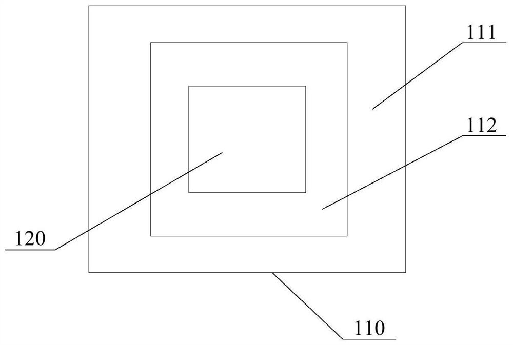
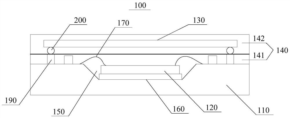
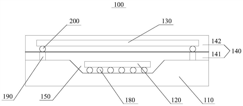
[0028] Such as figure 1 , figure 2 and image 3 As shown, one aspect of the present invention provides a multi-chip packaging structure 100 , including a substrate 110 , a first chip 120 , a second chip 130 and a plastic encapsulation layer 140 . The first chip 120 and the second chip 130 are sequentially stacked on the substrate 110, that is, as figure 2 As shown, the first chip 120 is disposed toward the substrate 110, the second chip 130 is disposed away from the substrate 110, and both the first chip 120 and the second chip 130 are electrically connected to the substrate 110. For example, the first chip 120 can be connected to the substrate 110 by wire bonding. The substrate 110 is electrically connected. In addi...


PUM


Abstract

The invention provides a multi-chip packaging structure and packaging method. The packaging structure comprises a substrate, a first chip, a second chip and a plastic packaging layer, wherein the first chip and the second chip are sequentially stacked on the substrate, the plastic packaging layer wraps the first chip and the second chip, and the first chip and the second chip are electrically connected with the substrate; the substrate comprises a wiring area located on the periphery of the substrate and a non-wiring area located in the middle of the substrate, the non-wiring area is provided with a groove, and the first chip is arranged in the groove. The first chip is accommodated in the groove arranged in the non-wiring area of the substrate, so that the size of the whole packaging structure can be effectively reduced. Besides, when the first chip is fixed in the groove through a bonding layer (generally adopting glue such as chip mounting glue and the like), the arranged groove can well control overflow of the chip mounting glue, so that when the first chip is electrically connected with the substrate in a lead bonding mode, the risk that a bonding lead cannot be hit can be effectively reduced, and meanwhile, the relative height of the bonding wire arc can be effectively reduced, and the cost is saved.

Description

technical field [0001] The invention belongs to the technical field of chip packaging, and in particular relates to a multi-chip packaging structure and packaging method. Background technique [0002] Multi-chip packaging and device miniaturization are the future development direction of semiconductor devices. Multi-chip packaging technology is a packaging process that can meet the requirements of integration density and improve the performance of the whole machine. Generally, it can be divided into 2D structural packaging and 3D structural packaging, each of which has its own advantages and disadvantages. In order to cater to the development trend of miniaturization and functionalization of electronic products, it is often necessary to integrate more than two chips, even passive components such as capacitors, resistors, and inductors, into a package structure with a limited area. [0003] At present, the common 3D structure stacking combination packaging scheme is that a ...

Claims


Application Information

Patent Timeline
IPC IPC(8): H01L25/07H01L23/10H01L23/13H01L21/50
CPCH01L25/071H01L23/10H01L23/13H01L25/50H01L2224/48091H01L2224/73265H01L2224/16225H01L2224/16235H01L2924/15153H01L2924/00014
Inventor 沈鹏飞邱胜峰
Owner 通富微电科技(南通)有限公司
Learn More