
Eureka
For R&D, Eureka makes reading and utilizing patents & technical documents easy.
Eureka AIR
Designed for self-driven R&D workflows. Generate viable solutions, solve complex R&D challenges, empower your innovation with AI.

Eureka Materials
Designed for material experts only. Revolutionize your material R&D, from search, analyze, to developing new materials.

TechResearch
Generate reliable direction feasibility study reports for your R&D in just a few steps.

TechSeek
Discover and master advanced knowledge NOW. Basics, ideas, possibilities, all at once.

TechMind
As an expert in R&D Theories, TechMind can generates customized viable solutions instantly.

TechRisk
Analyze your overall solution with one click, know your potential R&D risks in advance.

TechMonitor
Get weekly tech updates, stay abreast of the latest tech innovations and key insights.
TFT substrate structure and preparation method thereof
A substrate and glass substrate technology, applied in the field of TFT substrate structure and its preparation, to reduce costs and improve product yield
- Summary
- Abstract
- Description
- Claims
- Application Information
AI Technical Summary
Problems solved by technology
Method used
Image

Examples
preparation example Construction
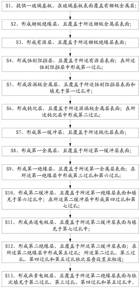
[0041] A method for preparing a TFT substrate structure, comprising the following steps:
[0042] S1. A glass substrate is provided, and the surface of the glass substrate is covered with a gate metal layer;
[0043] S2, forming a gate insulating layer and covering the surface of the gate metal layer;
[0044] S3, forming an active layer and covering the surface of the gate insulating layer;
[0045] S4, forming an etching barrier layer covering the surface of the active layer; forming a first via hole in the etching barrier layer;
[0046] S5, forming a source and drain metal layer, covering the surface of the etching barrier layer and filling in the first via hole;
[0047] S6, forming a passivation layer covering the surface of the source-drain metal layer; forming a second via hole in the passivation layer;
[0048] S7, forming a first buffer layer and covering the surface of the passivation layer;
[0049] S8, forming a first metal layer and covering the surface of the ...
Embodiment 1
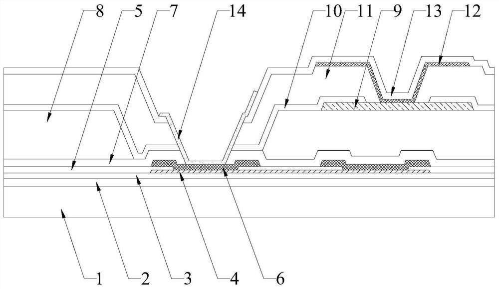
[0063] Please refer to figure 1 , Embodiment 1 of the present invention is:
[0064] Please refer to figure 1 , a TFT substrate structure, comprising a glass substrate 1, a gate metal layer 2, a gate insulating layer 3, an active layer 4, an etching stopper layer 5, a source and drain layer are sequentially stacked and covered on one side of the glass substrate 1 Pole metal layer 6, passivation layer 7, first buffer layer 8, first metal layer 9, first insulating layer 10, second buffer layer 11, common electrode layer 12 and second insulating layer 13, the etching barrier layer 5 is provided with a first via hole, the first via hole is filled with the source-drain metal layer 6, the passivation layer 7 is provided with a second via hole, and the first insulating layer 10 is provided with a first via hole. Three via holes, the second buffer layer 11 is provided with a fourth via hole, the second insulating layer 13 is provided with a fifth via hole, the second via hole, the t...
Embodiment 2
[0080] Please refer to figure 2 , the second embodiment of the present invention is:
[0081] A method for preparing a TFT substrate structure, comprising the following steps:
[0082] S1. Provide a glass substrate 1, the surface of the glass substrate 1 is covered with a gate metal layer 2;
[0083] S2, forming a gate insulating layer 3 and covering the surface of the gate metal layer 2;
[0084] S3, forming an active layer 4 and covering the surface of the gate insulating layer 3;
[0085] S4, forming an etching barrier layer 5, and covering the surface of the active layer 4; forming a first via hole in the etching barrier layer 5;
[0086] S5, forming the source-drain metal layer 6, and covering the surface of the etching barrier layer 5 and filling in the first via hole;
[0087] S6, forming a passivation layer 7 and covering the surface of the source-drain metal layer 6; forming a second via hole in the passivation layer 7;
[0088] S7, forming a first buffer layer ...
PUM
 Abstract
Description
Claims
Application Information
 - R&D Engineer
- R&D Manager
- IP Professional
- Industry Leading Data Capabilities
- Powerful AI technology
- Patent DNA Extraction
Browse by: Latest US Patents, China's latest patents, Technical Efficacy Thesaurus, Application Domain, Technology Topic, Popular Technical Reports.
© 2024 PatSnap. All rights reserved.Legal|Privacy policy|Modern Slavery Act Transparency Statement|Sitemap|About US| Contact US: help@patsnap.com