Wafer cleaning and drying method and mechanism

A drying method and wafer technology, applied in electrical components, semiconductor/solid-state device manufacturing, circuits, etc., can solve the problems of incomplete drying, discontinuous wafer movement, affecting the Marangoni effect, etc., to save drying space, The effect of improving the support method and shortening the overall stroke

Active Publication Date: 2021-09-03
HANGZHOU ZHONGGUI ELECTRONICS TECH CO LTD
View PDF4 Cites 2 Cited by
  • Summary
  • Abstract
  • Description
  • Claims
  • Application Information

AI Technical Summary

Problems solved by technology

At this time, if the positioning groove of the wafer is facing downward, the thimble structure must first complete the empty stroke generated by the part where the positioning groove is located, before continuing to push the wa

Method used


Image

  • Wafer cleaning and drying method and mechanism
  • Wafer cleaning and drying method and mechanism
  • Wafer cleaning and drying method and mechanism

Examples


Embodiment Construction

[0042] In order to enable those skilled in the art to better understand the solutions of the present invention, the technical solutions in the embodiments of the invention will be clearly and completely described below in conjunction with the drawings in the embodiments of the present invention. Obviously, the described embodiments are only It is a part of embodiments of the present invention, but not all embodiments. Based on the embodiments of the present invention, all other embodiments obtained by persons of ordinary skill in the art without making creative efforts shall fall within the protection scope of the present invention.

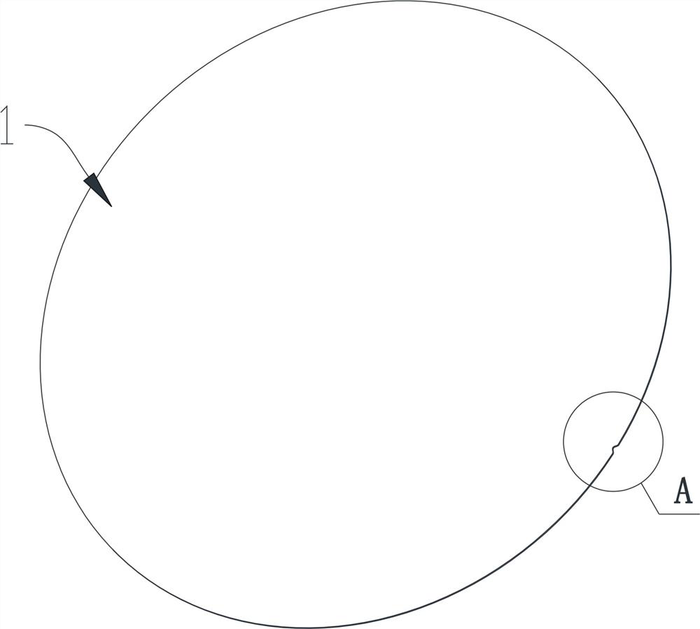
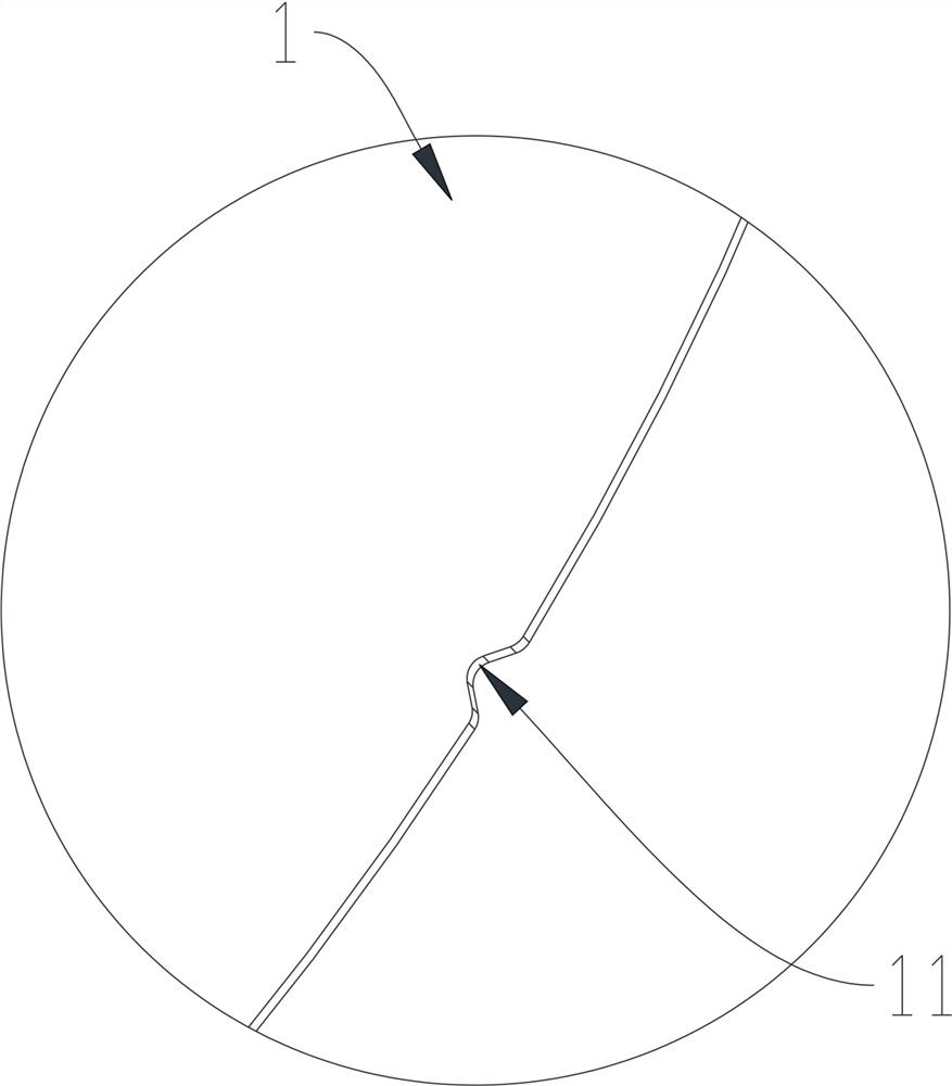
[0043] Such as Figure 1-Figure 2 As shown, a small positioning groove 11 is formed on the edge of the wafer 1 in order to help the subsequent process to determine the placement position of the wafer, and to achieve positioning for operations such as cutting and testing.

[0044] Such as Figure 2-Figure 11 As shown, a wafer cleaning and drying...


PUM


Abstract

The invention discloses a wafer cleaning and drying method which comprises the following steps: a wafer enters a box body and is completely immersed in cleaning liquid, and the bottom of the wafer is supported and limited by a fixed supporting seat; a horizontal limiting mechanism vertically moves upwards to limit swinging of the wafer; a pushing mechanism vertically moves upwards by a first stroke to be in contact with the wafer, and the first stroke is the distance between the pushing mechanism and the wafer; the pushing mechanism drives the wafer to move upwards, the horizontal limiting mechanism moves upwards cooperatively and keeps a contact state with the wafer so as to limit inclination of the wafer, the wafer continuously moves upwards to extend out of the liquid level, and a spraying mechanism sprays dry gas to the wafer; when the horizontal limiting mechanism approaches the liquid level, the horizontal limiting mechanism stops moving upwards, and at the moment, the pushing mechanism keeps moving upwards, so that continuous upward movement of the wafer is ensured until the wafer is completely separated from the cleaning liquid. The invention further discloses a wafer cleaning and drying mechanism. The wafer is in contact with the bottom propelling mechanism from the beginning of ascending, it is ensured that the wafer is always stressed and continuously sent out, and the cleaning effect is ensured.

Description

technical field [0001] The invention belongs to the technical field of semiconductor integrated circuit chip manufacturing, and in particular relates to a wafer cleaning and drying method and mechanism. Background technique [0002] Chemical mechanical planarization is a processing technology in integrated circuit technology. With the development of technology, the requirements for processing technology will increase accordingly. At the same time, chemical mechanical planarization is a wet process in the wafer processing process, and a large amount of polishing liquid and different chemical reagents will be used in the entire process. Therefore, At the end of the process, the wafer needs to be cleaned and dried to remove particles attached to the surface of the wafer, so that it can enter the next process. [0003] In the existing integrated circuit equipment, the traditional drying method is spin drying, which uses the centrifugal force generated at high speed to remove th...

Claims


Application Information

Patent Timeline
IPC IPC(8): H01L21/67H01L21/02
CPCH01L21/67057H01L21/67034H01L21/02057
Inventor 殷骐杨渊思顾海洋
Owner HANGZHOU ZHONGGUI ELECTRONICS TECH CO LTD
Why Eureka
Try Eureka