Supercharge Your Innovation With Domain-Expert AI Agents!

GGNMOS ESD protection device structure based on anti-radiation SOI technology

A technology for protecting devices and SOI, which is applied in semiconductor devices, electrical solid state devices, semiconductor/solid state device components, etc., can solve problems such as failure of integrated circuits, and achieve the effect of solving the problem of unstable breakdown voltage

Active Publication Date: 2021-09-03
58TH RES INST OF CETC
View PDF3 Cites 0 Cited by
  • Summary
  • Abstract
  • Description
  • Claims
  • Application Information

AI Technical Summary

Problems solved by technology

[0004] The object of the present invention is to provide a GGNMOS ESD protection device structure based on radiation-resistant SOI technology, so as to solve the current problem that ESD easily causes integrated circuit failure

Method used


Image

  • GGNMOS ESD protection device structure based on anti-radiation SOI technology
  • GGNMOS ESD protection device structure based on anti-radiation SOI technology
  • GGNMOS ESD protection device structure based on anti-radiation SOI technology

Examples


Embodiment 1

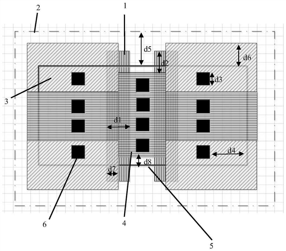
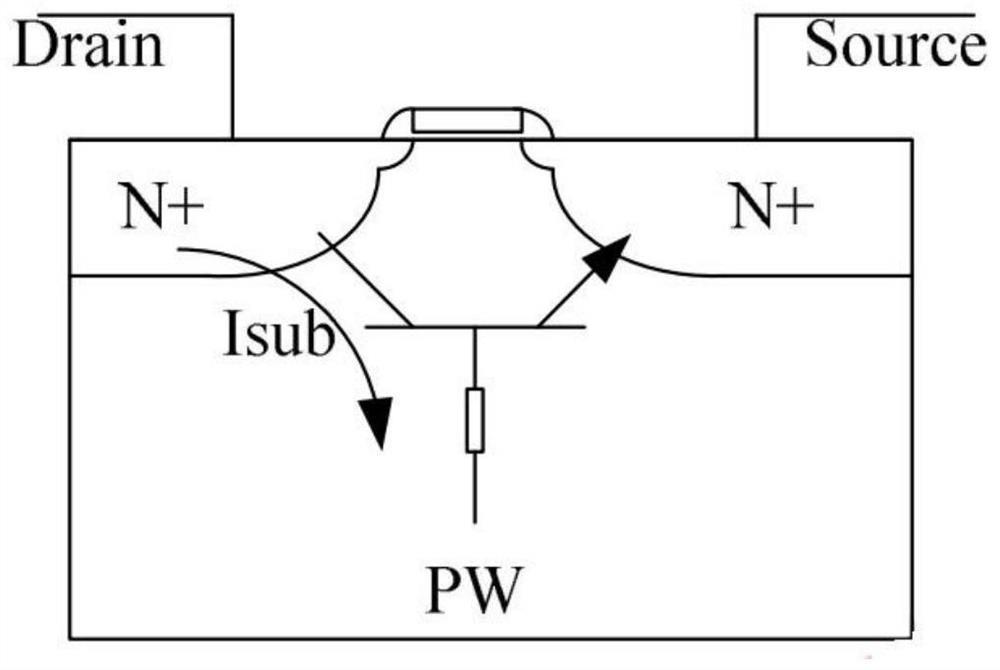
[0022] The invention provides a GGNMOS ESD protection device structure based on radiation-resistant SOI technology, its structure is as follows figure 1 As shown, it includes polycrystalline gate POLY layer 1, STI reinforcement injection layer 2, P-type body contact injection layer 3, N-type source-drain injection layer 4, active region TO layer 5 and contact hole W1 layer 6, and the N-type drain terminal The source-drain injection layer 4 is located in the active region TO layer 5 .

[0023] The polycrystalline gate POLY layer 1 is strip-shaped, and the N-type source-drain injection layer 4 is in the form of two back-to-back horizontal T-shaped layers, straddling two polycrystalline gate POLY layers 1 . The P-type body contact injection layer 3 is four rectangles, covering the four corners of the TO layer 5 in the active region and part of the polycrystalline POLY layer 1 . The TO layer 5 in the active region surrounds and maintains a distance from the N-type source-drain in...


PUM

PropertyMeasurementUnit
Bar widthaaaaaaaaaa

Abstract

The invention discloses a GGNMOSESD protection device structure based on an anti-radiation SOI process, and belongs to the field of semiconductor integrated circuits. According to the invention, the N-type source-drain injection layer is shrunk into the TO layer of the active region, the process is realized through photoetching, and the design can effectively solve the problems that the breakdown voltage of a protection device is unstable and the ESD resistance is reduced caused by an anti-radiation reinforcement injection process; through TLP test evaluation, the original structure of the reinforcement process is below 0.5 A, and the novel structure is above 2.5 A.

Description

technical field [0001] The invention relates to the technical field of semiconductor integrated circuits, in particular to a GGNMOS ESD protection device structure based on a radiation-resistant SOI process. Background technique [0002] ESD protection technology has been the focus of research in the field of microelectronics. According to statistics, failures caused by ESD account for more than 37% of integrated circuit failures, and this proportion is further increasing with the reduction of device feature size. [0003] The characteristics of high speed, low leakage, good sub-threshold characteristics, latch-up immunity and low soft error rate provided by SOI technology have made it one of the most competitive technologies widely used. Since the bottom of the SOI device is isolated by a thick buried oxide layer, and the surroundings of the device are also fully dielectrically isolated by SiO2, SOI devices and circuits are very sensitive to ESD stress on the one hand; on ...

Claims


Application Information

Patent Timeline
IPC IPC(8): H01L23/60H01L27/02
CPCH01L23/60H01L27/0266H01L27/0296H01L27/0292
Inventor 顾祥贺琪张庆东谢儒彬吴建伟
Owner 58TH RES INST OF CETC
Features
  • R&D
  • Intellectual Property
  • Life Sciences
  • Materials
  • Tech Scout
  • Unparalleled Data Quality
  • Higher Quality Content
  • 60% Fewer Hallucinations
Learn More