

3D-printed integrated digital micro-fluidic chip structure and manufacturing method thereof
A 3D printing and digital microfluidic technology, applied in the field of digital microfluidic technology and 3D printing, can solve the problems of slow molding speed, high failure rate, cumbersome chip manufacturing steps, etc.
- Summary
- Abstract
- Description
- Claims
- Application Information
AI Technical Summary
Problems solved by technology
Method used
Image


Examples
Embodiment 1
[0033] See attached figure 1 As shown, Embodiment 1 of the present invention provides a 3D printing integrated digital microfluidic chip structure. The digital microfluidic chip includes two parts: an upper plate 1 and a lower plate 2, and the upper plate 1 is a hydrophobic electrode; The lower plate 2 includes a base plate 21 , a dielectric layer 22 , a hydrophobic layer 23 and a 3D microstructure layer 24 connected in sequence; the base plate 21 includes a base layer 211 and an electrode layer 212 connected in sequence.
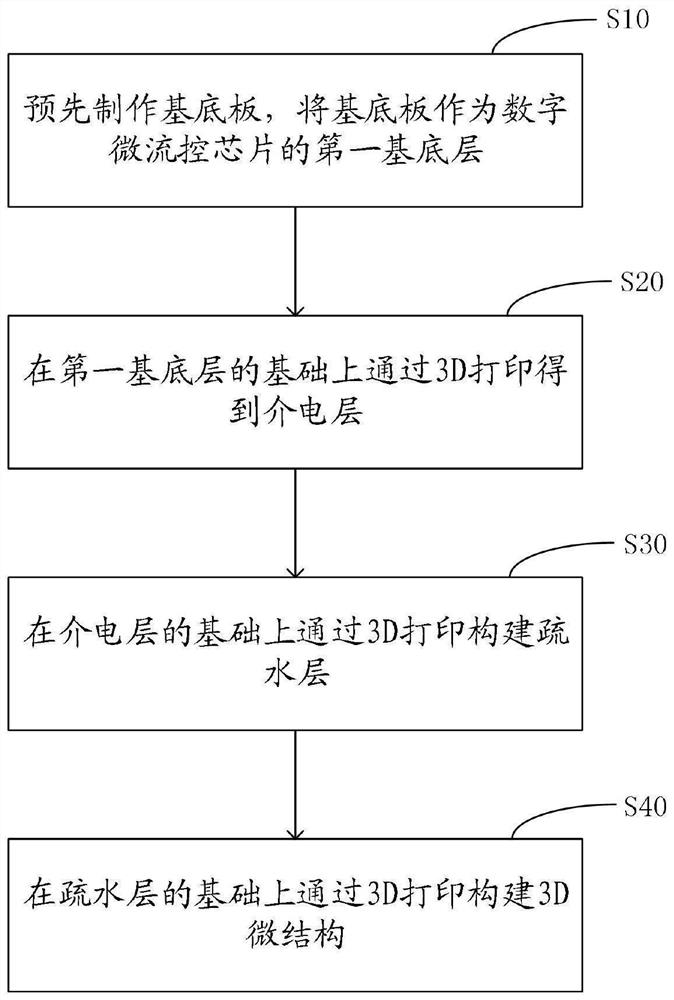
[0034] See attached figure 2 As shown, Embodiment 1 of the present invention also provides a method for manufacturing a 3D printed integrated digital microfluidic chip, including:
[0035] S10: prefabricating the base plate 21, using the base plate 21 as the first base layer of the digital microfluidic chip;
[0036] S20: obtaining the dielectric layer 22 by 3D printing on the basis of the first base layer 211;
[0037] S30: building a hydrophobic layer...
Embodiment 2
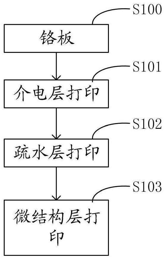
[0051] See attached image 3 As shown, the one-step manufacturing flow chart of the 3D printing dielectric layer and 3D microstructure layer provided in Example 2 includes the integrated manufacture of the dielectric layer 22, 3D microstructure layer and hydrophobic layer on the basis of the base plate and electrodes. Layer 23, the following describes the one-step manufacturing of the 3D printed dielectric layer and 3D microstructure layer, including the following operations:
[0052] S100: Prefabricate a chromium plate substrate of a certain size, and the chromium plate substrate layer is used as the lower substrate layer 211 of the digital microfluidic device to be manufactured by 3D printing;
[0053] S101: Deposit the first layer of photosensitive resin on the base layer 211 of the chromium plate by printing, as the dielectric layer 22 of the digital microfluidic chip, and the thickness of the dielectric layer 22 can be designed by yourself;
[0054] S102: build a hydroph...
Embodiment 3
[0059] See attached Figure 4 As shown, the integrated forming flow chart of the 3D printed digital microfluidic chip provided in Example 3, the entire digital microfluidic chip is printed in one step with a 3D printer, and the base layer of the chromium plate prefabricated in Example 2 is 3D printed Manufactured in the form of, the specific manufacturing steps are:
[0060] S200: Deposit a substrate with a certain thickness by printing as the substrate layer 211 of the electrode layer;
[0061] S201: Combining multi-material 3D printing technology to build an electrode structure on the base layer 211 to obtain a chromium plate base layer;
[0062] S202: Deposit the first layer of photosensitive resin on the base layer of the chrome plate by printing, as the dielectric layer 212 of the digital microfluidic chip, and the thickness of the dielectric layer 212 can be designed by yourself;
[0063] S203: build a hydrophobic layer 23 on the dielectric layer 212 according to a set...
PUM
 Abstract
Description
Claims
Application Information