

Method for forming film layer with uniform thickness distribution and semiconductor structure
A technology of thickness distribution and film layer, applied in semiconductor devices, semiconductor/solid-state device manufacturing, transistors, etc., can solve problems such as uneven film thickness, breakdown, leakage, etc.
- Summary
- Abstract
- Description
- Claims
- Application Information
AI Technical Summary
Problems solved by technology
Method used
Image

Examples
Embodiment Construction
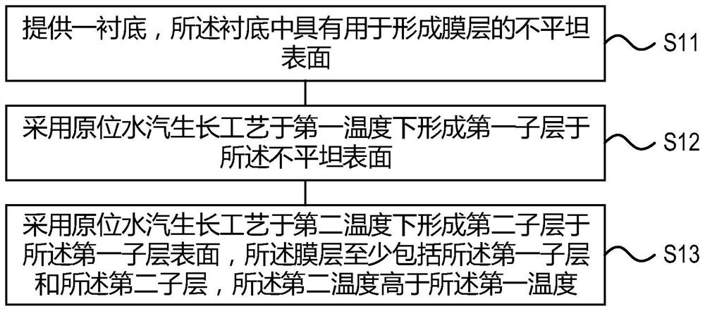
[0033] The method for forming a film with uniform thickness distribution and the specific implementation of the semiconductor structure provided by the present invention will be described in detail below with reference to the accompanying drawings.
[0034] This specific embodiment provides a method for forming a film layer with uniform thickness distribution, with figure 1 It is a flow chart of a film layer forming method with uniform thickness distribution in the specific embodiment of the present invention, with Figures 2A-2F It is a schematic cross-sectional view of the main process in the process of forming a film layer with uniform thickness distribution in the specific embodiment of the present invention. like figure 1 , Figures 2A-2F As shown, the method for forming a film layer with uniform thickness distribution provided by this specific embodiment includes the following steps:
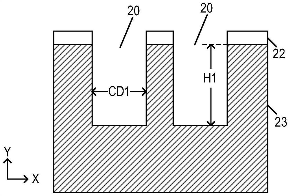
[0035] In step S11, a substrate 23 is provided, and the substrate 23 has an uneven ...
PUM
| Property | Measurement | Unit |
|---|---|---|
| thickness | aaaaa | aaaaa |
Abstract
Description
Claims
Application Information