Electronic component packaging structure of IML touch film and manufacturing method of electronic component packaging structure

A technology of electronic components and packaging structures, which is applied to the assembly of printed circuits with electrical components, electrical components, and printed circuit manufacturing. It can solve the problems of IML touch film burns, open circuits, and complex repair methods.

Pending Publication Date: 2021-09-14
深圳市合盛创杰科技有限公司
View PDF0 Cites 0 Cited by
  • Summary
  • Abstract
  • Description
  • Claims
  • Application Information

AI Technical Summary

Problems solved by technology

[0003] The current IML touch film technology usually uses SMT technology to mount electronic components on the conductive ink layer. Specifically, the electronic components are soldered to the IML touch film through solder paste. However, tin After the paste is cured, it is relatively fragile. In the subsequent processes such as stretching and molding, the solder paste welding position is prone to cracking, resulting in poor contact or even open circ

Method used


Image

  • Electronic component packaging structure of IML touch film and manufacturing method of electronic component packaging structure
  • Electronic component packaging structure of IML touch film and manufacturing method of electronic component packaging structure
  • Electronic component packaging structure of IML touch film and manufacturing method of electronic component packaging structure

Examples


Embodiment Construction

[0028] In order to have a clearer understanding of the technical features, purposes and effects of the present invention, the specific implementation manners of the present invention will now be described in detail with reference to the accompanying drawings.

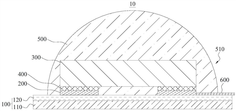
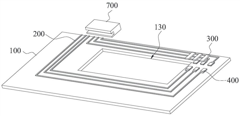
[0029] figure 1 Shown is an electronic component packaging structure of an IML touch film in an embodiment of the present invention, the package structure includes an IML touch film body 100 , a conductive circuit layer 200 , electronic components 300 and a conductive colloid 400 . The conductive circuit layer 200 is disposed on the main body 100 of the IML touch film, and the conductive circuit layer 200 plays a role of transmitting electric current. The pins of the electronic component 300 are connected to the conductive circuit layer 200 through the conductive colloid 400, and the electronic component 300 is used for electrification. The conductive colloid 400 is respectively connected to the pins of the electronic ...


PUM


Abstract

The invention discloses an electronic component packaging structure of an IML touch film and a manufacturing method of the electronic component packaging structure. The packaging structure comprises an IML touch film main body, a conductive circuit layer, an electronic component and a conductive glue body; the conductive circuit layer is arranged on the IML touch film main body; a pin of the electronic component is connected with the conductive circuit layer through the conductive glue body. According to the electronic component packaging structure of the IML touch film, the electric connection between the electronic component and the conductive circuit layer is realized by using the conductive glue body, so that the connection reliability between the electronic component and the conductive circuit layer is improved; cracking and separation of the connection position of the electronic component and the conductive circuit layer in the subsequent working procedures such as stretching forming are avoided as much as possible, and the yield of the IML touch film is increased; in addition, the electronic component can be connected to the conductive circuit layer at a low temperature, the IML touch film is prevented from being scalded due to too high temperature in the installation process of the electronic component; and the arrangement of a decorative layer wave thin film is omitted, and the production cost is reduced.

Description

technical field [0001] The invention relates to the technical field of IML touch film, in particular to an electronic component packaging structure of an IML touch film and a manufacturing method thereof. Background technique [0002] The existing IML touch film is relatively popular in the in-mold injection molding industry due to its many advantages such as good touch sensitivity, free design, simple assembly, light weight, and high-tech sense. [0003] The current IML touch film technology usually uses SMT technology to mount electronic components on the conductive ink layer. Specifically, the electronic components are soldered to the IML touch film through solder paste. However, tin After the paste is cured, it is relatively fragile. In the subsequent processes such as stretching and molding, the solder paste welding position is prone to cracking, resulting in poor contact or even open circuit; [0004] Secondly, in the actual soldering process, since the curing tempera...

Claims


Application Information

Patent Timeline
IPC IPC(8): H05K1/18H05K3/32
CPCH05K1/181H05K3/321H05K2201/10106H05K2203/1316
Inventor 艾建华王三刚
Owner 深圳市合盛创杰科技有限公司
Why Eureka
Try Eureka