

Air intake and exhaust structure of semiconductor chamber and semiconductor chamber
A technology of air intake and exhaust and semiconductor, which is applied in semiconductor/solid-state device manufacturing, crystal growth, electrical components, etc. It can solve the problems affecting the thickness uniformity and sudden change of film deposition on wafers, so as to optimize the thickness uniformity and speed up the flow rate , The effect of easy disassembly and assembly
- Summary
- Abstract
- Description
- Claims
- Application Information
AI Technical Summary
Problems solved by technology
Method used
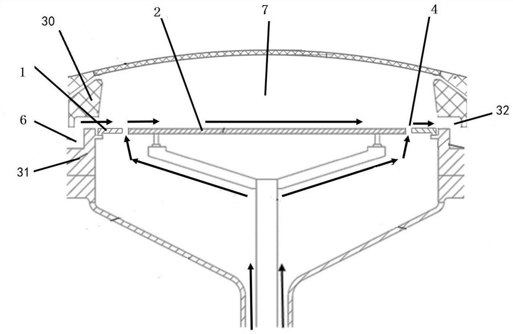
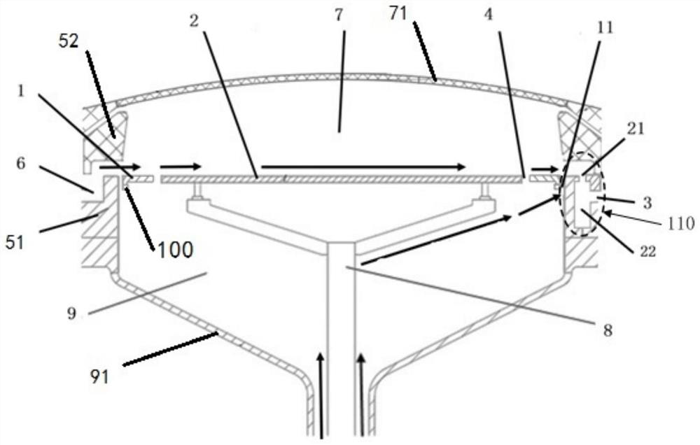
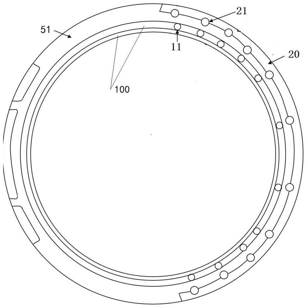
Image

Examples
Embodiment Construction
[0033] The present invention will be described in more detail below. While the present invention has provided preferred embodiments, it should be understood that the invention can be embodied in various forms and should not be limited by the embodiments set forth herein. Rather, these embodiments are provided so that this disclosure will be thorough and complete, and will fully convey the scope of the invention to those skilled in the art.
[0034] In the description of the present invention, it should be noted that the terms "center", "upper", "lower", "left", "right", "vertical", "horizontal", "inner", "outer" etc. The indicated orientation or positional relationship is based on the orientation or positional relationship shown in the drawings, and is only for the convenience of describing the present invention and simplifying the description, rather than indicating or implying that the referred device or element must have a specific orientation, or in a specific orientation....
PUM
 Abstract
Description
Claims
Application Information